SOI CMOS radio frequency switch with high voltage resistance

A radio frequency switch, high withstand voltage technology, applied in the direction of electronic switches, electrical components, pulse technology, etc., can solve the problem of insufficient power carrying capacity of radio frequency switches, and achieve the effect of improving power carrying capacity

Pending Publication Date: 2022-02-11
江苏乾合微电子有限公司
View PDF0 Cites 0 Cited by
  • Summary
  • Abstract
  • Description
  • Claims
  • Application Information

AI Technical Summary

Problems solved by technology

[0005] In view of the deficiencies in the background technology, the present invention provides a high withstand voltage SOI CMOS radio frequency switch, and the technical problem to be solved is that the power carrying capacity of the existing radio frequency switch is insufficient

Method used


Image

  • SOI CMOS radio frequency switch with high voltage resistance
  • SOI CMOS radio frequency switch with high voltage resistance
  • SOI CMOS radio frequency switch with high voltage resistance

Examples


Embodiment 1

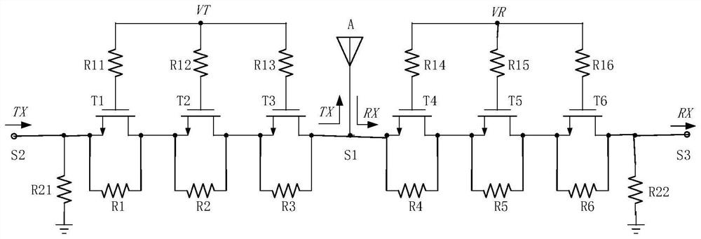
[0022] like figure 2 As shown, the radio frequency switch in this embodiment includes an emission channel and a receiving channel. The main path of the transmit channel is from the three switches t1 to T3 of the terminal 2 S2 until the terminal one S1, and the transmit signal Tx moves to the antenna. The main path of the receiving channel is from the three switch tanks T4 to T6 from the terminal one S1 until the terminal three S3, and the received signal RX leaves the antenna. The switch tubes T1 to T6 are all implemented using the SOI CMOS process, such as NMOS devices. A resistor R1, a resistor R2, a compensation capacitor C2, a resistor R3, a compensation capacitor C1 and a resistor R4, a resistor R5, a resistor R6, respectively, a compensation capacitor C1 and a resistor R4, a resistor R5, and a resistor R6, respectively. The gate of the switches t1 to t3 on the main path of the transmit channel is connected to the control voltage a VT by one resistor R11 to R13, respectively....

Embodiment 2

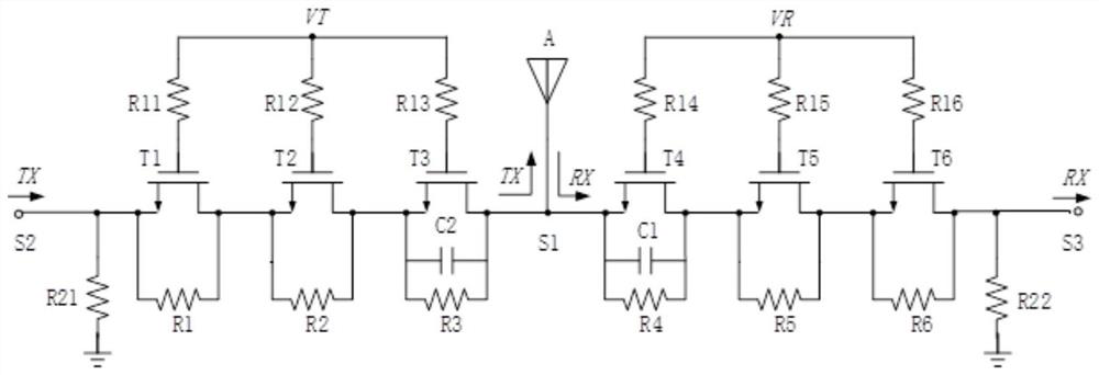
[0026] figure 2 When the radio frequency switch is used, if the RF signal power level of the S2 port is improved, the T5 switch tube T5 will reach the T6 tube to the upper limit of its source drain voltage, which in turn makes the switch tube T5 first breakdown. In view of this, if image 3 As shown, the radio frequency switch in this embodiment includes an emission channel and a receiving channel. The main path of the transmit channel is from the three switches t1 to T3 of the terminal 2 S2 until the terminal one S1, and the transmit signal Tx moves to the antenna. The main path of the receiving channel is from the three switch tanks T4 to T6 from the terminal one S1 until the terminal three S3, and the received signal RX leaves the antenna. The switch tubes T1 to T6 are all implemented using the SOI CMOS process, such as NMOS devices. A resistor R1, a compensation capacitor C4 and a resistor R2, a compensation capacitor C1 and a resistor R3, a compensation capacitor C1 and a res...

Embodiment 3

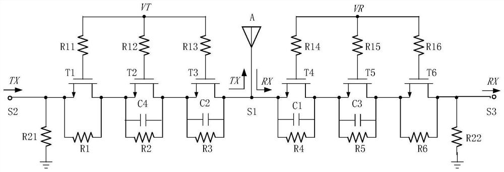
[0030] The radio frequency switch in the first and seconds can not only be used to switch the emission channel and the reception channel, or it can be used to switch any two channels. See Figure 4 This is a deformed structure of Example 2, schematically with radio frequency signals Tx1 and Tx2 of two different emission channels. Figure 4 The radio frequency switch shown includes a channel one with a channel 2. The main path of the channel is from the three switches t1 to T3 of the terminal two S2 until the terminal one S1, and the signal is transferred to the antenna. The main path of the channel 2 is from the three switch tanks T4 to T6 from the terminal three S3 until the terminal one S1, and the signal two Tx2 moves to the antenna. Figure 4 The principle of implementation of the frequency switches image 3 The displayed frequency switches are the same, and will not be described again.

[0031]In an embodiment from one to three, the main path of each passage is only coupled to th...


PUM


Abstract

The invention relates to the technical field of radio frequency switches, and discloses a capacitance compensation type SOI CMOS radio frequency switch. The switch comprises a fixed end and at least one selection end, wherein a channel is formed between each selection end and the fixed end; the main path of each channel is M cascaded switch tubes, the grid electrodes of the switch tubes of each channel are connected with the same control voltage, a resistor is connected between the source electrode and the drain electrode of each switch tube, each channel selects N continuous switch tubes from the fixed end, capacitors are respectively connected between the source electrodes and the drain electrodes of the N continuous switch tubes, and the capacitors between the source electrodes and the drain electrodes of the switch tubes are connected with the resistors between the drain electrodes and the source electrodes of the switch tubes in parallel. In the actual use, the capacitors between the source electrodes and the drain electrodes of the N continuous switch tubes can enable radio frequency signals to be uniformly distributed on the switch tubes on the closed channel, so the switch tubes on the closed channel are prevented from being broken down due to uneven voltage distribution, and the power bearing capacity of the whole radio frequency switch is further improved.

Description

Technical field [0001] The present invention relates to the technical field of radio frequency switches, and more particularly to a high voltage SOI CMOS radio frequency switch. Background technique [0002] In the field of mobile communication technology, the mobile terminal is often provided with a plurality of RF power amplifiers, each radio frequency power amplifier, and each radio frequency power amplifier, often provided in the mobile terminal. Only a signal enlarged by a plurality of frequency bands close to a frequency band or frequency range is enlarged, and the desired RF power amplifier is switched to the corresponding path using a RF switch. [0003] Refer figure 1 , figure 1 The radio frequency switch shown includes an emission channel and a receiving channel. The main path of the transmit channel is from the three switches t1 to T3 of the terminal 2 S2 until the terminal one S1, and the transmit signal Tx moves to the antenna. The main path of the receiving channel ...

Claims


Application Information

Patent Timeline
Patent Type & Authority Applications(China)
IPC IPC(8): H03K17/041H03K17/687
CPCH03K17/041H03K17/687
Inventor 赵鹏
Owner 江苏乾合微电子有限公司
Why Eureka
Try Eureka