Semiconductor device and read method of NAND flash memory

一种闪速存储器、半导体的技术,应用在静态存储器、只读存储器、数字存储器信息等方向,能够解决读出时间变长、影响感测节点、恢复时间花费较长等问题,达到高可靠性读出动作、高速读出读出动作的效果

Pending Publication Date: 2022-02-18
WINBOND ELECTRONICS CORP
View PDF12 Cites 0 Cited by
  • Summary
  • Abstract
  • Description
  • Claims
  • Application Information

AI Technical Summary

Problems solved by technology

If the recovery time of the sensing node is longer, the readout time will be longer, which will affect the voltage of the sensing node for sensing the memory cells after the NAND string is discharged, so it is necessary to restore the original voltage more accurately

Method used


Image

  • Semiconductor device and read method of NAND flash memory
  • Semiconductor device and read method of NAND flash memory
  • Semiconductor device and read method of NAND flash memory

Examples


Embodiment Construction

[0023] The semiconductor storage device of the present invention is, for example, a NAND-type flash memory or a microprocessor, microcontroller, logic, application specific integrated circuit (ASIC) embedded in such a flash memory, or an image or sound processing device. A processor, a processor that processes signals such as wireless signals, and the like. In the following description, a NAND-type flash memory is exemplified. In an embodiment of the present invention, in order to realize the interchangeability of the NOR flash memory, the NAND flash memory is equipped with a serial peripheral interface (Serial Peripheral Interface, SPI), and has an external clock signal. Simultaneous and continuous readout of multiple pages.

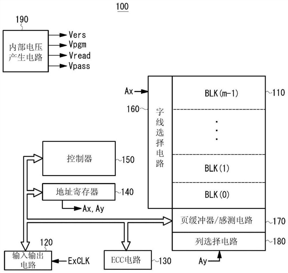
[0024] figure 1It is a figure which shows the structure of the NAND type flash memory which concerns on the Example of this invention. The flash memory 100 of the present embodiment includes the following components: a memory cell array 110, in which...


PUM


Abstract

A semiconductor device and a read method of a NAND flash memory capable of performing high-speed read or high-reliability read are provided. The read method of a NAND flash memory includes: a pre-charging step of pre-charging a sensing node via a voltage-supply node; a discharging step of discharging a voltage of the sensing node to the voltage-supply node to perform a prescribed operation; a recharging step of recharging the sensing node via the voltage-supply node after the prescribed operation; and a read step of discharging a NAND string and performing sensing of a memory cell.

Description

technical field [0001] The present invention relates to a method of reading a NAND flash memory of a semiconductor device including a NAND flash memory, and more particularly, to a recovery method of a sensing node of a page buffer / sense circuit. Background technique [0002] A NAND-type flash memory is equipped with a continuous read function (burst read function) for continuously reading out a plurality of pages in response to an external command. A page buffer / sensing circuit includes, for example, two latches, and in a continuous read operation, one latch can output the other latch while data read from the array is held in the other latch. data held in the device (for example, Japanese Patent No. 5323170, Japanese Patent No. 5667143, US Patent Application US2014 / 0104947A1, etc.). [0003] In the read operation of the NAND type flash memory, in order to receive the charge from the sensing node more accurately, the latch of the page buffer needs to be reset, and the reset...

Claims


Application Information

Patent Timeline
Patent Type & Authority Applications(China)
IPC IPC(8): G11C16/26G11C16/24G11C7/12G11C7/10
CPCG11C16/26G11C16/24G11C7/12G11C7/1057G11C7/106G11C7/1048G11C16/32G11C16/0483G11C2211/5643G11C2211/5642G11C16/10G11C16/30
Inventor 冈部翔妹尾真言
Owner WINBOND ELECTRONICS CORP
Why Eureka
Try Eureka