Supercharge Your Innovation With Domain-Expert AI Agents!

Array substrate and manufacturing method thereof

A technology for array substrates and manufacturing methods, which is applied in the direction of electrical components, electrical solid devices, circuits, etc., can solve problems such as easy peeling of film layers, low production yield, and decreased product reliability, so as to improve peeling phenomena and improve production. Yield rate, effect of increasing adhesion

Pending Publication Date: 2022-03-11
SHENZHEN CHINA STAR OPTOELECTRONICS TECH CO LTD
View PDF0 Cites 0 Cited by
  • Summary
  • Abstract
  • Description
  • Claims
  • Application Information

AI Technical Summary

Problems solved by technology

[0004] The embodiment of the present application provides an array substrate and a method for manufacturing the array substrate, so as to solve the problem that the film layer of the existing array substrate is prone to peeling off, resulting in a decrease in product reliability and a low production yield.

Method used


Image

  • Array substrate and manufacturing method thereof
  • Array substrate and manufacturing method thereof
  • Array substrate and manufacturing method thereof

Examples


Embodiment Construction

[0034] The technical solutions in the embodiments of the present application will be clearly and completely described below in conjunction with the drawings in the embodiments of the present application. Apparently, the described embodiments are only some of the embodiments of this application, not all of them. Based on the embodiments in this application, all other embodiments obtained by those skilled in the art without making creative efforts belong to the protection scope of this application.

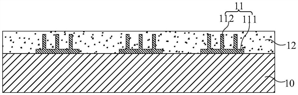
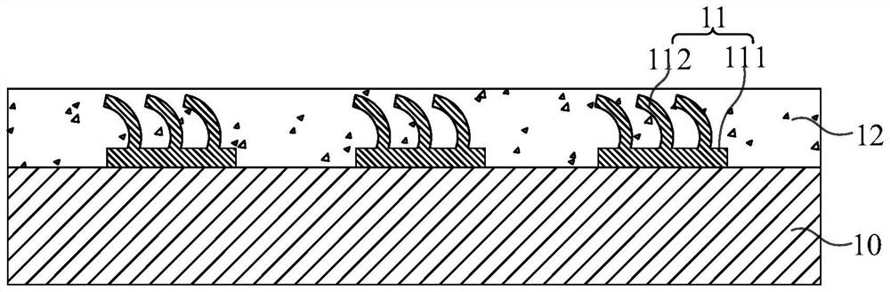
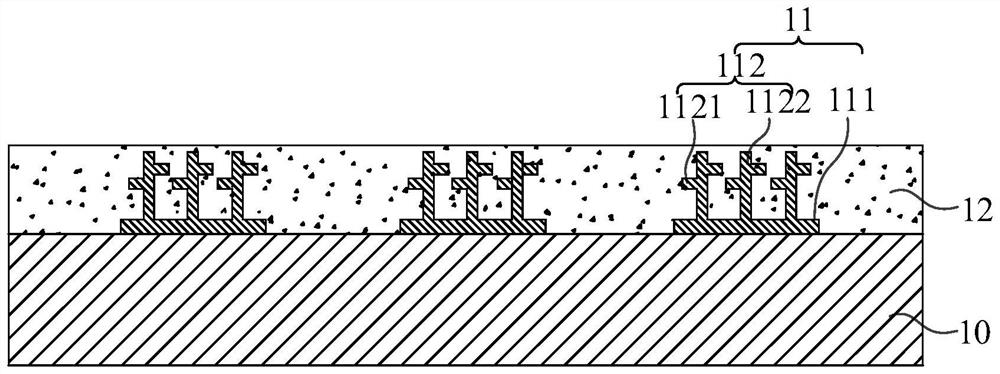
[0035] For the existing array substrates, due to the large size, complex film layers and numerous manufacturing processes, the film layer is prone to fall off from the substrate or the upper film layer and the lower film layer are peeled off during the production process, resulting in low production yield. The present invention securely locks the film layer and the substrate or different film layers together by means of a micromechanical lock structure, so as to improve the peeling ...


PUM


Abstract

The embodiment of the invention provides an array substrate and a manufacturing method of the array substrate. The array substrate comprises a substrate; the lock accessory is connected with the base plate; the first film layer is arranged on the substrate, and at least part of the lock accessory is embedded into the first film layer, so that the lock accessory can fix the first film layer. According to the array substrate provided by the embodiment of the invention, the lock accessory is arranged on the substrate, and at least part of the lock accessory is embedded into the first film layer, so that the adhesive force between the lock accessory and the first film layer is further increased, the peeling phenomenon of the film layer of the array substrate can be effectively improved, the production yield is improved, and the production cost is reduced.

Description

technical field [0001] The present invention relates to the field of display technology, in particular to an array substrate and a manufacturing method of the array substrate. Background technique [0002] With the development of display technology, display panels are widely used in various consumer electronic products such as mobile phones, televisions, personal digital assistants, and notebook computers, and become the mainstream of display devices. The display panel has multi-layer film layers, and the multi-layer film layers constitute the functional layers of the display panel, any problem in any layer will cause the display panel to malfunction. [0003] The base layer PI, light-shielding layer BM, photoresist layer PS, organic film layer PFA, etc. of the display panel are usually coated on the array substrate by liquid photoresist, and then patterned by a yellow light process. As the size of the array substrate continues to increase, the requirements for the thicknes...

Claims


Application Information

Patent Timeline
IPC IPC(8): H01L27/32
CPCH10K59/124
Inventor 邵源
Owner SHENZHEN CHINA STAR OPTOELECTRONICS TECH CO LTD
Features
  • R&D
  • Intellectual Property
  • Life Sciences
  • Materials
  • Tech Scout
  • Unparalleled Data Quality
  • Higher Quality Content
  • 60% Fewer Hallucinations
Learn More