Wafer detection data processing method and computer readable storage medium

A technology for detecting data and processing methods, applied in the field of wafer manufacturing, which can solve the problems of low efficiency of wafer failure bit detection and achieve the effect of improving efficiency

Pending Publication Date: 2022-03-15
CHANGXIN MEMORY TECH INC
View PDF0 Cites 0 Cited by
  • Summary
  • Abstract
  • Description
  • Claims
  • Application Information

AI Technical Summary

Problems solved by technology

[0005] The purpose of the present disclosure is to provide a method for processing wafer detection data and a computer-readable storage medium, at least to a certain extent, to overcome the problem of low detection efficiency of wafer failure bits in the related art

Method used


Image

  • Wafer detection data processing method and computer readable storage medium
  • Wafer detection data processing method and computer readable storage medium
  • Wafer detection data processing method and computer readable storage medium

Examples


Embodiment Construction

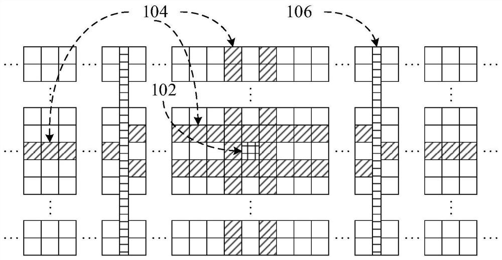
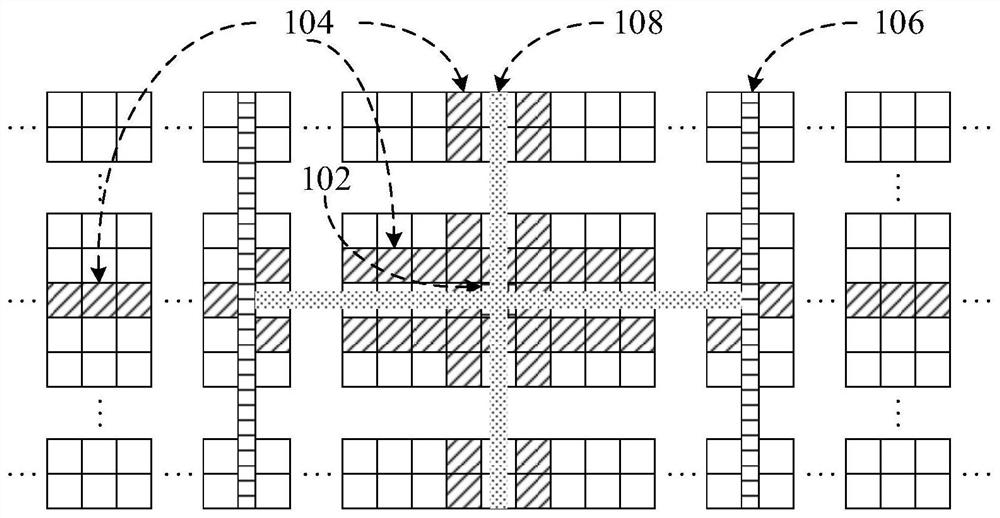
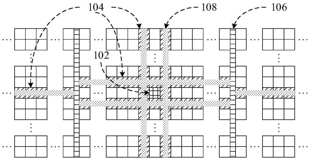
[0034] Example embodiments will now be described more fully with reference to the accompanying drawings. Example embodiments may, however, be embodied in many forms and should not be construed as limited to the examples set forth herein; rather, these embodiments are provided so that this disclosure will be thorough and complete and will fully convey the concept of example embodiments to those skilled in the art. The described features, structures, or characteristics may be combined in any suitable manner in one or more embodiments.

[0035] Furthermore, the drawings are merely schematic illustrations of the present disclosure and are not necessarily drawn to scale. The same reference numerals in the drawings denote the same or similar parts, and thus repeated descriptions thereof will be omitted. Some of the block diagrams shown in the drawings are functional entities and do not necessarily correspond to physically or logically separate entities. These functional entities ...


PUM


Abstract

The invention provides a wafer detection data processing method and a computer readable storage medium, and relates to the technical field of wafer manufacturing. The wafer detection data processing method comprises the following steps: determining a new failure bit generated in a completed wafer detection process; obtaining a repair record of the new invalid bit and a repair record of an adjacent bit of the new invalid bit; the repair record is analyzed to determine attribute information of the new failure bit and the adjacent bit, and the attribute information comprises at least one of position information, standby circuit information, a unit graph of the new failure bit and a wafer detection process; performing classified learning according to the attribute information to obtain a failure bit prediction model; and predicting a failure bit to be subjected to wafer detection through the failure bit prediction model. According to the technical scheme, the reliability of failure bit prediction is improved, and the yield of wafer products can be improved.

Description

technical field [0001] The present disclosure relates to the technical field of wafer manufacturing, and in particular to a method for processing wafer detection data and a computer-readable storage medium. Background technique [0002] In the stage of wafer probing (circuit probing), all the positions of Fail Bits (hereinafter referred to as FBs) will be repaired, and this disclosure refers to the repair of FBs as "general repair". [0003] In addition, some non-FBs positions may also be repaired. In the multi-pass test program after "general repair", new invalid bits may appear in non-FBs positions. Therefore, these non-FBs positions will be repaired together after the general repair, which is called "predictive repair". [0004] Most of the circuit wiring on the wafer is at the micron or nanometer level. To determine the failure bit by manual screening or probe unit-by-unit elimination will not only lead to low efficiency of wafer detection and affect the yield of wafer ...

Claims


Application Information

Patent Timeline
Patent Type & Authority Applications(China)
IPC IPC(8): G06F30/392G06K9/62G06F111/14
CPCG06F30/392G06F2111/14G06F18/241G11C29/38G11C29/4401G11C29/785G11C29/18G11C29/006
Inventor 仰蕾陈予郎
Owner CHANGXIN MEMORY TECH INC
Why Eureka
Try Eureka