Device and method for detecting comprehensive defects of silicon carbide wafer

A technology of defect detection and silicon carbide, applied in the direction of transmittance measurement, scattering characteristic measurement, etc., can solve the problems of chip scratches, reduce the efficiency of chip detection, reduce the quality of the chip, etc., achieve accurate positioning, and facilitate the effect of chip quality analysis

Pending Publication Date: 2022-04-05
BEIJING TIANKE HEDA SEMICON CO LTD
View PDF0 Cites 0 Cited by
  • Summary
  • Abstract
  • Description
  • Claims
  • Application Information

AI Technical Summary

Problems solved by technology

However, most of the optical inspection equipment on the market has specificity in defect detection, that is, it can only detect one or several defects.
If you want to detect all the defects of silicon carbide wafers, you need to send the wafers to different optical inspection equipment for inspection separately, which will introduce additional time and capital costs, and it is easy to cause scratches on the wafers when transferring the wafers, thereby reducing the quality of the wafers
And many optical inspection equipment are manual or semi-automatic, that is, after the wafer is placed in the optical instrument, it is necessary to manually find the defect position, and after the defect is found, it is necessary to manually take pictures and record and process the data, which undoubtedly reduces the efficiency of wafer inspection

Method used


Image

  • Device and method for detecting comprehensive defects of silicon carbide wafer
  • Device and method for detecting comprehensive defects of silicon carbide wafer

Examples


Embodiment Construction

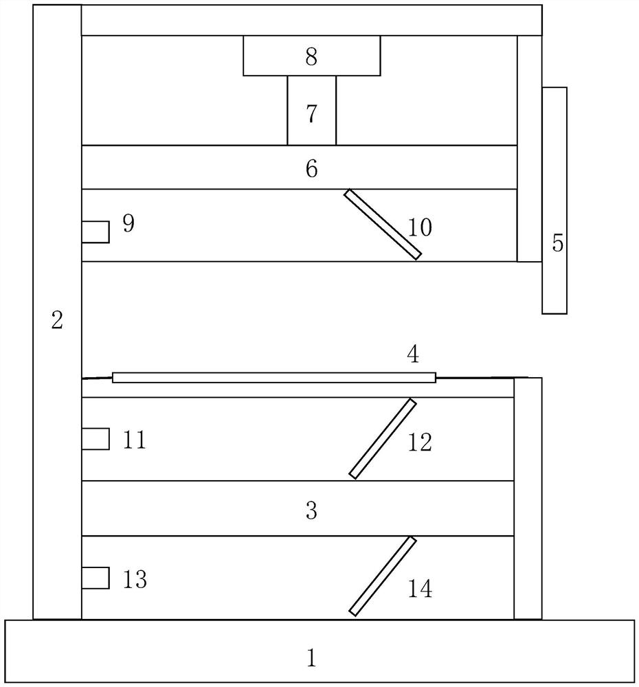
[0058] The patented invention has simple structure, high degree of automation and strong versatility, can accurately and quickly detect various defects in silicon carbide wafers, and automatically collect defect statistics.

[0059]The following will clearly and completely describe the technical solutions in the embodiments of the present invention with reference to the accompanying drawings in the embodiments of the present invention. Obviously, the described embodiments are only some, not all, embodiments of the present invention. Based on the embodiments of the present invention, all other embodiments obtained by persons of ordinary skill in the art without making creative efforts belong to the protection scope of the present invention.

[0060] The present invention adopts following technical scheme:

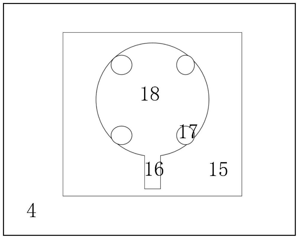
[0061] A comprehensive defect detection device for silicon carbide wafers, which simply adopts an optical detection method and has an auto-focus function, and can simultaneo...


PUM

PropertyMeasurementUnit
speedaaaaaaaaaa
transmittivityaaaaaaaaaa
luminanceaaaaaaaaaa

Abstract

According to the comprehensive defect detection device and method for the silicon carbide wafer, an optical detection method is purely adopted, an automatic focusing function is added, and multiple defects on the front face, the back face and the interior of the silicon carbide wafer can be detected at the same time through multi-photosynthetic use; and statistical information of various defects of the silicon carbide wafer is automatically identified and collected in cooperation with an intelligent algorithm program. By adopting the method, various defects of the silicon carbide wafer can be quickly, accurately and automatically identified and counted, and the various defects can be accurately positioned, so that the quality analysis of the wafer is facilitated.

Description

technical field [0001] The invention relates to the technical field of silicon carbide, in particular to a comprehensive defect detection device and method for a silicon carbide wafer. Background technique [0002] Silicon carbide has a wide band gap, high thermal conductivity and high breakdown voltage, making it widely used in devices that work at high frequency, high power, radiation resistance, and extreme conditions. It is a kind of semiconductor material with great potential. [0003] Defect-free silicon carbide wafers are critical to fabricate high-quality epitaxial wafers, which in turn determine the performance of semiconductor devices. Common silicon carbide wafer defects include micropipes, pits, scratches, chipping, miscellaneous crystals, and wrapping. Therefore, defect detection of the produced silicon carbide wafers is an important step to ensure the quality of silicon carbide products. [0004] In recent years, people have mastered a variety of methods for...

Claims


Application Information

Patent Timeline
Patent Type & Authority Applications(China)
IPC IPC(8): G01N21/47G01N21/49G01N21/59
Inventor 郭钰刘春俊张世颖柴海帅王波彭同华杨建
Owner BEIJING TIANKE HEDA SEMICON CO LTD
Why Eureka
Try Eureka