Chip packaging structure, forming method and electronic equipment

A chip packaging structure, chip technology, applied in the direction of circuits, electrical components, phonon exciters, etc., can solve the problems that the epoxy resin cavity cannot meet the airtightness requirements, low integration, large substrate packaging volume, etc.

Pending Publication Date: 2022-04-08
SHANGHAI JUYOU SMART INTELLIGENCE TECH CO LTD
View PDF0 Cites 0 Cited by
  • Summary
  • Abstract
  • Description
  • Claims
  • Application Information

AI Technical Summary

Problems solved by technology

[0004] In view of this, the present application provides a chip packaging structure, forming method and electronic equipment to solve the problem that the existing chip requires airtightness and exposure at the same time, the volume of the substrate package is large, the integration degree is low, and the epoxy resin The problem that the cavity cannot meet the airtightness requirements

Method used


Image

  • Chip packaging structure, forming method and electronic equipment
  • Chip packaging structure, forming method and electronic equipment
  • Chip packaging structure, forming method and electronic equipment

Examples


Embodiment Construction

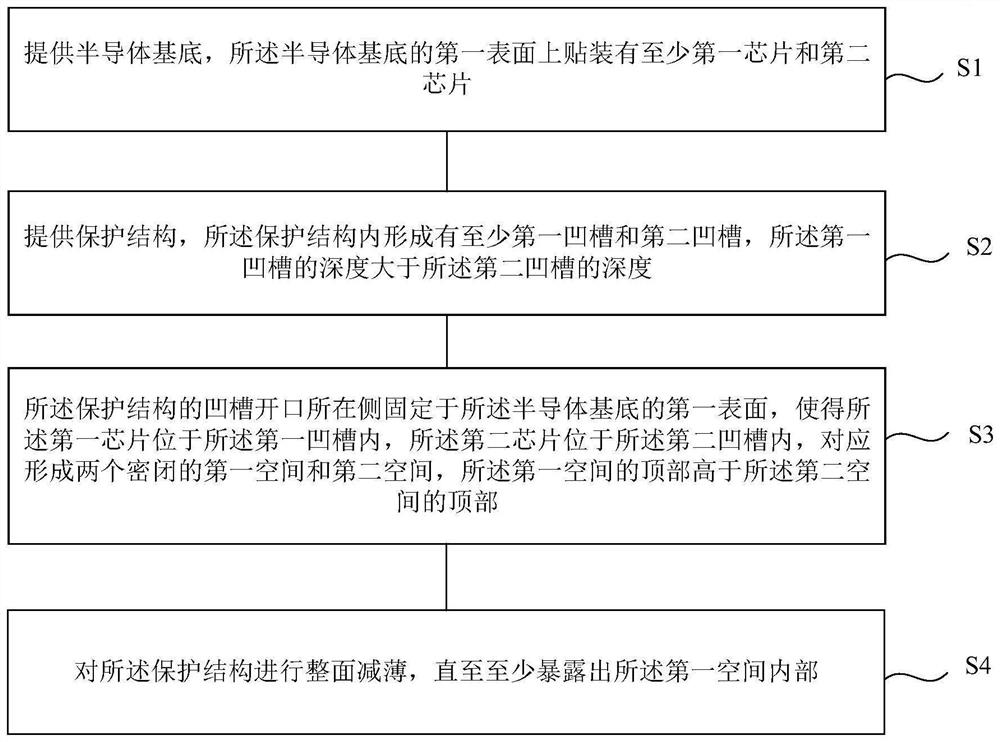
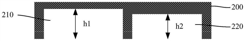
[0031] As mentioned in the background technology, in the prior art, epoxy resin cofferdams are usually used to form a specific airtight space on the PCB substrate during packaging, and a specific exposure area is formed through a glass cover to meet the airtightness of the chip. sex and exposure requirements. The chip integration realized by the substrate process has a large package volume and a low integration level, and the epoxy resin cavity cannot meet the airtightness requirements. To this end, the inventor proposes a new method for forming a chip packaging structure, through a semiconductor substrate and a protective structure, the protective structure includes at least a first space and a second space, the first space is a first groove, and the The second space is an airtight cavity, the first depth from the bottom of the first groove to the opening is greater than the second depth from the bottom to the top in the airtight cavity; the first chip is located in the first...


PUM


Abstract

The invention discloses a chip packaging structure, a forming method and electronic equipment, the packaging structure comprises a semiconductor substrate, and at least a first chip and a second chip are mounted on the first surface of the semiconductor substrate; the protection structure is located on the first surface of the semiconductor substrate and comprises at least a first space and a second space, the first space is a first groove, the second space is a closed cavity, and a first depth from the bottom of the first groove to an opening is larger than a second depth from the bottom to the top in the closed cavity; the first chip is located at the bottom of the first groove, and the second chip is located at the bottom of the closed cavity. By means of the first groove with the first depth larger than the second depth and the closed cavity, the first chip located in the first groove can be exposed to achieve light transmission, and meanwhile the second chip with the requirement for air tightness is still located in the closed cavity to meet the air tightness requirement.

Description

technical field [0001] The present application relates to the field of semiconductor packaging, in particular to a chip packaging structure, forming method and electronic equipment. Background technique [0002] With the increasing integration of electronic chips, the complexity of chip packaging continues to increase. Chips with different functions have different requirements for packaging. Some chips have higher requirements for airtightness and require airtight packaging, while some chips require better exposure and need to be exposed. [0003] In the prior art, for chips that require airtightness and exposure at the same time, epoxy resin cofferdams are usually used to form a specific airtight space on the PCB (Printed Circuit Board, printed circuit board) when packaging, and pass The glass cover forms a specific exposure area to meet the requirements of chip airtightness and exposure. The chip integration realized by the substrate process has a large package volume an...

Claims


Application Information

Patent Timeline
IPC IPC(8): H01S5/02315H01S5/02345H01S5/0237H01S5/0239H01S5/026
Inventor 任玉龙柳鹏
Owner SHANGHAI JUYOU SMART INTELLIGENCE TECH CO LTD
Why Eureka
Try Eureka