FT test system and method for RF chip

A test system and chip technology, which is applied in the field of FT test system of RF chips, can solve the problems of increasing capital and time costs of IC design companies, tight use of machines, and scarce quantities, so as to save money and time costs and ensure accurate testing sexual effect

Pending Publication Date: 2022-04-12
KTD ELECTRONICS
View PDF0 Cites 0 Cited by
  • Summary
  • Abstract
  • Description
  • Claims
  • Application Information

AI Technical Summary

Problems solved by technology

[0004] This kind of dedicated RF chip testing machine is expensive (generally tens of millions or even hundreds of millions of RMB) and the quantity is scarce, entrusting packaging and testing manufacturers to test costs is high, and when the chip test is busy, the use of the machine will be relatively tight. If the test is queued, it is easy to cause delays in delivery, which will greatly increase the capital and time costs of IC design companies

Method used


Image

  • FT test system and method for RF chip
  • FT test system and method for RF chip
  • FT test system and method for RF chip

Examples


Embodiment Construction

[0036] It should be noted that the following detailed description is exemplary and intended to provide further explanation of the present invention. Unless defined otherwise, all technical and scientific terms used herein have the same meaning as commonly understood by one of ordinary skill in the art to which this invention belongs.

[0037] It should be noted that the terminology used here is only for describing specific embodiments, and is not intended to limit exemplary embodiments according to the present invention. As used herein, unless the context clearly indicates otherwise, the singular is intended to include the plural, and it should also be understood that when the terms "comprises" and / or "comprises" are used in this specification, it indicates that there are features, steps, operations, components and / or combinations thereof.

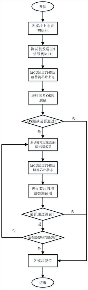
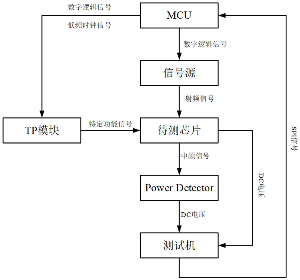
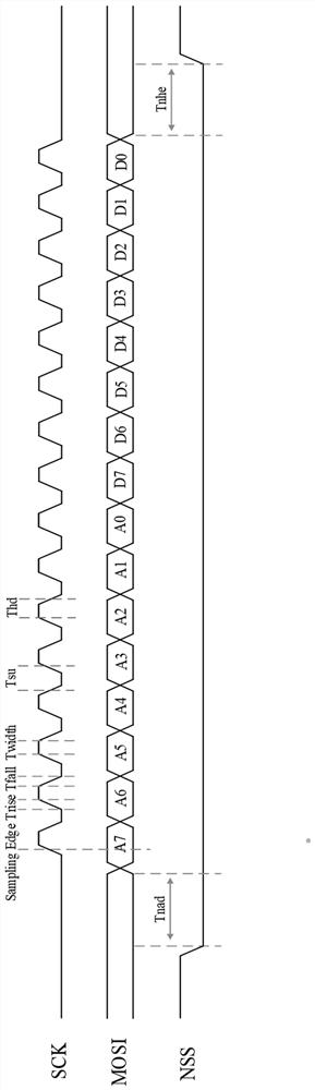
[0038] Such as Figure 1-Figure 4 As shown, the present invention discloses an FT test system for RF chips, which includes an MCU modul...


PUM


Abstract

The invention relates to an FT test system of an RF chip. The FT test system comprises an MCU module, a signal source module, a TP module, a chip to be tested, a Power Detector and a DC test machine. The DC test machine is in communication connection with the MCU module and is used for transmitting a control instruction to the MCU module; and the MCU module is connected with the TP module and the signal source module, outputs a digital logic signal and a low-frequency clock signal to the TP module according to a control instruction transmitted by the DC test machine, and outputs the digital logic signal to the signal source module to control the switching of the signal source module and the frequency of the output signal. According to the invention, the FT test work of the RF chip can be carried out without using a special RF chip test machine, and a large amount of fund and time cost can be saved on the premise of ensuring the test accuracy.

Description

technical field [0001] The invention relates to the field of RF chip testing, in particular to an FT testing system and method for RF chips. Background technique [0002] The RF chip is an electronic component that converts radio signal communication into a certain radio signal waveform and sends it out through antenna resonance. Compared with general power chips, in mass-production FT testing, in addition to various OS tests on RF chips, gain testing is also required. [0003] At present, the test machine used for FT testing of RF chips usually needs an external radio frequency signal generator, and the radio frequency signal is input into the chip under test through the Cable line, and then the chip under test will also pass the frequency conversion amplified signal through the Cable Line input testing machine, by comparing the properties of the two signals before and after, you can judge whether the function of the chip is qualified. [0004] This kind of dedicated RF c...

Claims


Application Information

Patent Timeline
Patent Type & Authority Applications(China)
IPC IPC(8): G01R31/28
Inventor 王建钦吴鑫龙陈榕朱陈星
Owner KTD ELECTRONICS
Why Eureka
Try Eureka