Supercharge Your Innovation With Domain-Expert AI Agents!

Chip input and output pin direction control circuit structure

A technology of input-output and direction control, applied in circuits, electrical components, electric solid-state devices, etc., can solve problems such as difficult development, low production efficiency, and long development time, so as to reduce development difficulty and development time, and improve production efficiency , the effect of high flexibility

Pending Publication Date: 2022-04-12
上海聪链信息科技有限公司
View PDF0 Cites 0 Cited by
  • Summary
  • Abstract
  • Description
  • Claims
  • Application Information

AI Technical Summary

Problems solved by technology

[0002] In multi-chip cascade design, data can be sent from the first chip to the lower chip in sequence, or vice versa, starting from the last chip to send data to the upper chip in sequence. Therefore, the same pin of the chip needs to be both As an input, it can also be used as an output. At present, the wiring outside the chip is used to achieve this purpose. The wiring structure is more complicated, and the development time is longer and the development is more difficult, resulting in lower production efficiency.

Method used


Image

  • Chip input and output pin direction control circuit structure

Examples


Embodiment Construction

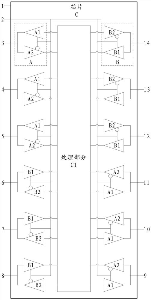
[0011] The embodiment of this specification provides a chip input and output pin direction control circuit structure, including a plurality of first input and output pins, a plurality of second input and output pins, a plurality of first control parts A, a plurality of second control parts B and the control pin.

[0012] like figure 1 As shown, taking chip C as an example, it has 1 power supply pin (No. 1), 1 control pin (No. 2), 6 first input and output pins (No. 3, No. 4, No. 5, 9 No., No. 10, No. 11), 6 second input and output pins (No. 6, No. 7, No. 8, No. 12, No. 13, No. 14), and 6 first input and output pins processed by chip C Part C1 is connected to 6 second input and output pins, among which, No. 3 pin corresponds to No. 14 pin. When No. 3 pin is used as input, it will be output by No. 14 pin after being processed by processing part C1; When the No. pin is used as input, it will be output by No. 3 pin after being processed by the processing part C1. Similarly, No. 4...


PUM


Abstract

A chip input and output pin direction control circuit structure comprises a plurality of first input and output pins and a plurality of second input and output pins corresponding to the first input and output pins, and the first input and output pins are connected with the second input and output pins through a processing part of a chip. Each first input and output pin is connected with the processing part through a first control piece, each second input and output pin is connected with the processing part through a second control piece, the control piece composed of two three-state gates is arranged on each input and output pin in the chip, one three-state gate is effective at a low level, the other three-state gate is effective at a low level, and the other three-state gate is effective at a low level. One three-state gate is effective at high level, the other three-state gate is effective at high level, when low level is input, the input and output pins can be used as input, and when high level is input, the input and output pins can be used as output, so that complex wiring outside a chip is not needed, the development difficulty and the development time are reduced, the production efficiency is improved, and the flexibility is high.

Description

technical field [0001] The invention relates to the field of chip technology, in particular to a circuit structure for controlling the direction of input and output pins of a chip. Background technique [0002] In multi-chip cascade design, data can be sent from the first chip to the lower chip in sequence, or vice versa, starting from the last chip to send data to the upper chip in sequence. Therefore, the same pin of the chip needs to be both As an input, it can also be used as an output. At present, the wiring outside the chip is used to achieve this purpose. The wiring structure is more complicated, and the development time is longer and the development is more difficult, resulting in lower production efficiency. Contents of the invention [0003] Based on this, aiming at the above technical problems, a chip input and output pin direction control circuit structure is provided. [0004] In order to solve the problems of the technologies described above, the present inv...

Claims


Application Information

Patent Timeline
Patent Type & Authority Applications(China)
IPC IPC(8): H01L27/118
Inventor 罗亦鸣时应超
Owner 上海聪链信息科技有限公司
Features
  • R&D
  • Intellectual Property
  • Life Sciences
  • Materials
  • Tech Scout
  • Unparalleled Data Quality
  • Higher Quality Content
  • 60% Fewer Hallucinations
Learn More