PWM signal dimming circuit and method for three-phase AC-powered LED lamps
A PWM signal, LED lamp technology, applied in the use of semiconductor lamps, electrical components and other directions, can solve the problems of reducing cost, not giving convenience, etc., to achieve the effect of convenient use, convenient dimming, and high reliability
- Summary
- Abstract
- Description
- Claims
- Application Information
AI Technical Summary
Problems solved by technology
Method used
Image
Examples
Embodiment 1
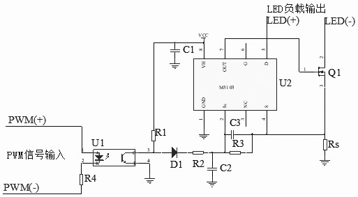
[0054] like figure 1 As shown in the figure, the basic way of realizing the dimming function in this embodiment is: after the external PWM signal is input through the isolation optocoupler circuit, after passing through the input impedance matching circuit, a dimming signal voltage is generated and provided to the driving chip circuit, and the driving chip circuit The output of the MOS transistor switch circuit is controlled according to the change of the dimming signal voltage and the change of the current signal collected by the LED load circuit, and the MOS transistor switch circuit controls the power change of the LED load circuit. Specifically: when the duty cycle of the PWM signal of the external dimming controller becomes larger, after the isolation optocoupler circuit and the input impedance matching circuit, the dimming signal voltage collected by the dimming control pin Is of the driver chip U2 becomes larger , the output voltage of the output power control pin OUT o...
Embodiment 2
[0056] like figure 2 As shown, in this embodiment, the pins of the driver chip U2 are defined as follows: pin 1 is the negative terminal of the power supply, grounded, pin 2 is the dimming control pin, which is connected to the resistor and capacitor, and pin 3 is floating, which is an empty tube Pin 4 is the current sampling pin, which is connected to the current sampling resistor and controlled by pin 2. The 5 pin of the driver chip U2 is the load output pin, and the 6 pin of the driver chip U2 is floating, which is an empty pin, the driver chip Pin 7 of U2 is the output control pin, and pin 8 of the driver chip U2 is the positive end of the power supply, which is connected to VCC.
[0057] The type of isolation optocoupler U1 is PC817, the driver chip U2 is M3103 of Hefei Yunshan Optoelectronics Technology Co., Ltd., the type of diode D1 is 1N4001, the type of MOS transistor Q1 is 1N80, the resistance value of resistor R1 is 1K ohm, the resistance value of resistor R2 is 1...
Embodiment 3
[0059]Similar to the above two embodiments, in this embodiment, a PWM signal dimming method and circuit for a three-phase 380V tunnel LED lamp driver chip interface, including an isolation optocoupler U1, a driver chip U2, a diode D1, a MOS Transistor Q1, resistor R1, resistor R2, resistor R3, resistor R4, resistor Rs, capacitor C1, capacitor C2, capacitor C3, etc. The pin 1 of the isolated optocoupler U1 is connected to the positive phase of the external PWM signal input PWM, the pin 2 of the isolated optocoupler U1 is connected to one end of the resistor R4, and the other end of the resistor R4 is connected to the negative phase of the external PWM signal input PWM , the pin 3 of the isolation optocoupler U1 is connected to the 8th pin of the driver chip U2 through the resistor R1, and is connected to the positive end of the diode D1 at the same time, and the pin 4 of the isolation optocoupler U1 is connected to the power ground. The negative end of the diode D1 is connected...
PUM
 Abstract
Description
Claims
Application Information

