Supercharge Your Innovation With Domain-Expert AI Agents!

Wafer pre-alignment method and device, electronic equipment and storage medium

A technology for storage media and wafers, applied in image data processing, instruments, calculations, etc., can solve problems such as low alignment accuracy, image distortion, and low wafer testing efficiency, and achieve the effect of improving alignment accuracy and efficiency

Pending Publication Date: 2022-04-19
精芯智能装备(苏州)有限公司
View PDF0 Cites 0 Cited by
  • Summary
  • Abstract
  • Description
  • Claims
  • Application Information

AI Technical Summary

Problems solved by technology

[0003] The current pre-alignment method for wafers is to use a line-scan camera to obtain the entire image of the wafer to achieve pre-alignment. Due to serious image distortion, the alignment accuracy of the pre-alignment process using a line-scan camera is low, which leads to Wafer test efficiency is low

Method used


Image

  • Wafer pre-alignment method and device, electronic equipment and storage medium
  • Wafer pre-alignment method and device, electronic equipment and storage medium
  • Wafer pre-alignment method and device, electronic equipment and storage medium

Examples


Embodiment Construction

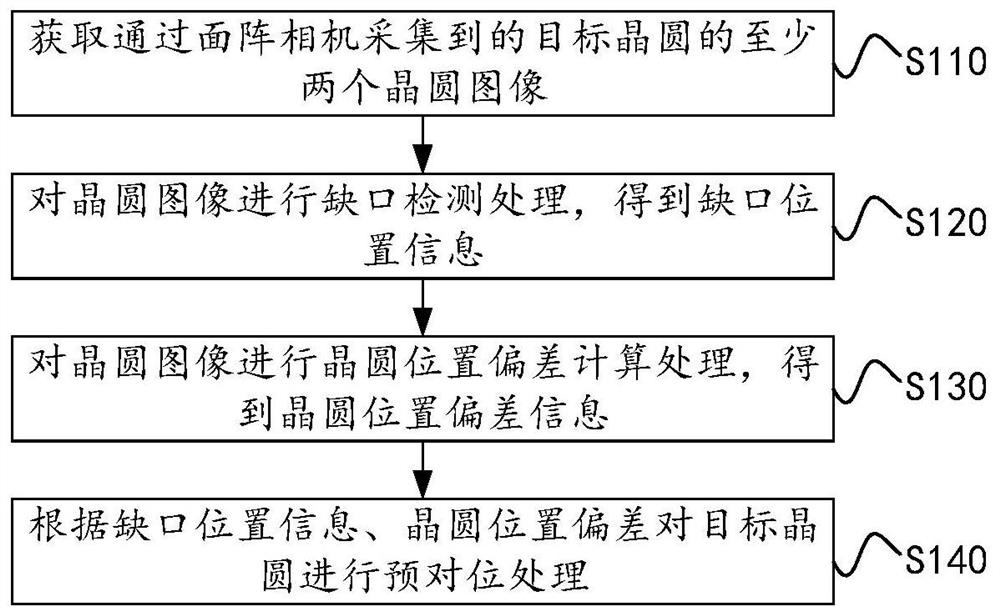
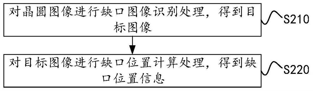
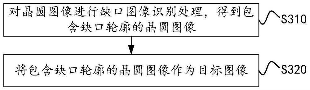
[0053] In order to make the object, technical solution and advantages of the present invention clearer, the present application will be further described in detail below in conjunction with the accompanying drawings and embodiments. It should be understood that the specific embodiments described here are only used to explain the present application, not to limit the present application.

[0054] It should be noted that although the functional modules are divided in the schematic diagram of the device, and the logical sequence is shown in the flowchart, in some cases, it can be executed in a different order than the module division in the device or the flowchart in the flowchart. steps shown or described. The terms "first", "second" and the like in the specification and claims and the above drawings are used to distinguish similar objects, and not necessarily used to describe a specific sequence or sequence.

[0055] Unless otherwise defined, all technical and scientific terms...


PUM


Abstract

The embodiment of the invention provides a wafer pre-alignment method and device, electronic equipment and a storage medium, and relates to the technical field of integrated circuit test equipment. The wafer pre-alignment method comprises the following steps: acquiring at least two wafer images of a target wafer acquired by an area-array camera; performing gap detection processing on the wafer image to obtain gap position information; performing wafer position deviation calculation processing on the wafer image to obtain wafer position deviation information; and performing pre-alignment processing on the target wafer according to the gap position information and the wafer position deviation information. According to the technical scheme provided by the embodiment of the invention, the wafer test efficiency can be improved.

Description

technical field [0001] The invention relates to the technical field of integrated circuit testing equipment, in particular to a wafer pre-alignment method and device, electronic equipment, and a storage medium. Background technique [0002] Wafer pre-alignment is one of the important functions of wafer testing equipment. The wafer must be pre-aligned to detect the center position and notch direction of the wafer before probe testing or optical inspection, so as to adjust the position and angle of the wafer. , so that the position and angle of the wafer on the test station meet the requirements. [0003] The current pre-alignment method for wafers is to use a line-scan camera to obtain the entire image of the wafer to achieve pre-alignment. Due to serious image distortion, the alignment accuracy of the pre-alignment process using a line-scan camera is low, which leads to Wafer testing is less efficient. Contents of the invention [0004] The main purpose of the embodiment...

Claims


Application Information

Patent Timeline
IPC IPC(8): G06T7/00G06T7/62G06T7/73
CPCG06T7/0008G06T7/73G06T7/62G06T2207/10004G06T2207/30148
Inventor 谢世高马海威王玮盛宇陶靖飞
Owner 精芯智能装备(苏州)有限公司
Features
  • R&D
  • Intellectual Property
  • Life Sciences
  • Materials
  • Tech Scout
  • Unparalleled Data Quality
  • Higher Quality Content
  • 60% Fewer Hallucinations
Learn More