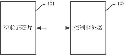
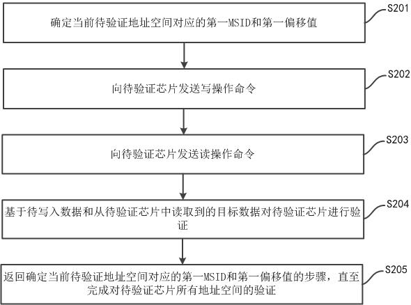
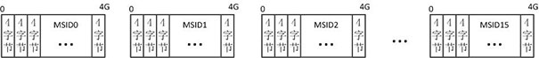
A chip verification method, device, system, control server and medium
A technology for controlling a server and a verification method, applied in the field of devices, systems, chip verification methods, control servers and media, can solve the problems of wasting manpower, unable to cover the address range of the chip, and taking a long time to achieve the effect of reducing manpower
- Summary
- Abstract
- Description
- Claims
- Application Information
AI Technical Summary
Problems solved by technology
Method used
Image

Examples
Embodiment Construction
[0071] The technical solutions in the embodiments of the present invention will be clearly and completely described below with reference to the accompanying drawings in the embodiments of the present invention. Obviously, the described embodiments are only a part of the embodiments of the present invention, but not all of the embodiments. Based on the embodiments of the present invention, all other embodiments obtained by those of ordinary skill in the art based on the present application fall within the protection scope of the present invention.
[0072] Different verification platforms may be used for the prototype verification of different modules of the chip and the entire chip system level. For example, the verification platform can be electronic design automation (Electronic design automation, EDA), simulation (emulation) or Field Programmable Gate Array (Field Programmable Gate Array). Array, FPGA). Among them, EDA is mainly used for module-level or small-system-level c...
PUM
 Abstract
Description
Claims
Application Information
 - R&D
- Intellectual Property
- Life Sciences
- Materials
- Tech Scout
- Unparalleled Data Quality
- Higher Quality Content
- 60% Fewer Hallucinations
Browse by: Latest US Patents, China's latest patents, Technical Efficacy Thesaurus, Application Domain, Technology Topic, Popular Technical Reports.
© 2025 PatSnap. All rights reserved.Legal|Privacy policy|Modern Slavery Act Transparency Statement|Sitemap|About US| Contact US: help@patsnap.com