Formation method of semiconductor structure
A semiconductor and graphic technology, applied in semiconductor/solid-state device manufacturing, electrical components, circuits, etc., can solve the problems of increasing the difficulty and complexity of integrated circuits, poor performance of semiconductor structures, etc., to reduce bridging, improve integrity and accuracy , the effect of improving performance
- Summary
- Abstract
- Description
- Claims
- Application Information
AI Technical Summary
Problems solved by technology
Method used
Image

Examples
Embodiment Construction
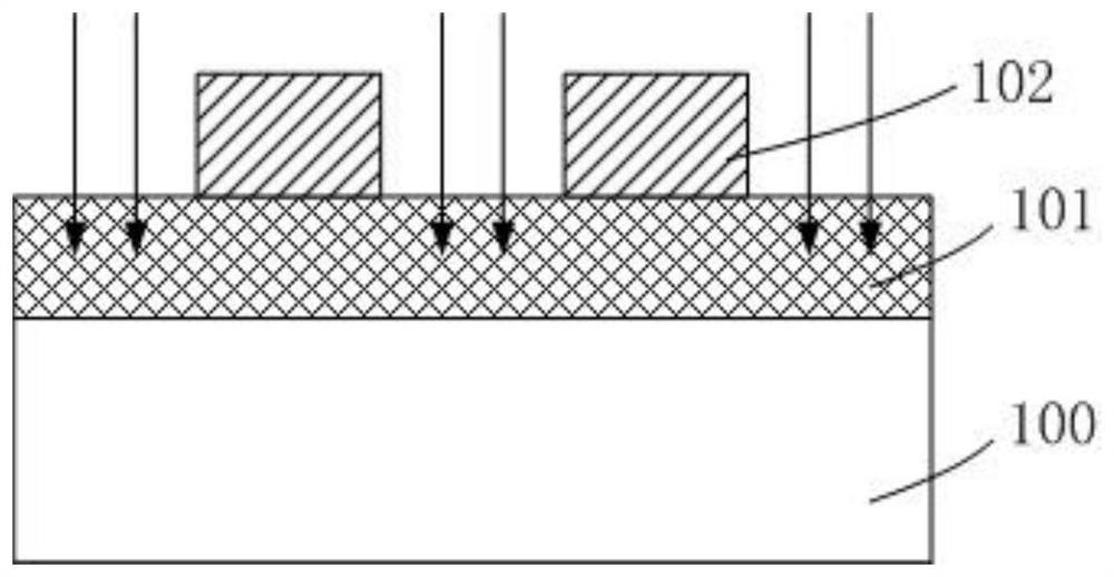
[0027] It can be seen from the background art that the performance of the current semiconductor structure is relatively poor. The reasons for the poor performance of the semiconductor structure are now analyzed in conjunction with the specific drawings.
[0028] refer to figure 1 , providing a layer to be etched 100; forming a sacrificial layer 101 on the layer to be etched 100; forming a first patterned layer 102 on the sacrificial layer 101, and the first patterned layer 102 exposes part of the sacrificial layer the surface of the layer 101; performing ion implantation on the exposed sacrificial layer.
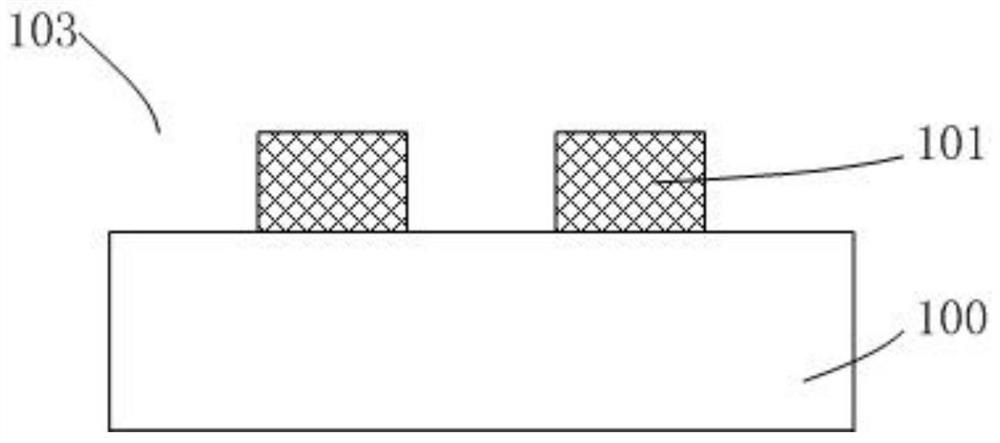
[0029] refer to figure 2 , remove the first patterned layer 102; remove the sacrificial layer 101 implanted with ions, and form a first opening 103 in the remaining sacrificial layer 101, and the first opening 103 exposes the layer to be etched 100 s surface.
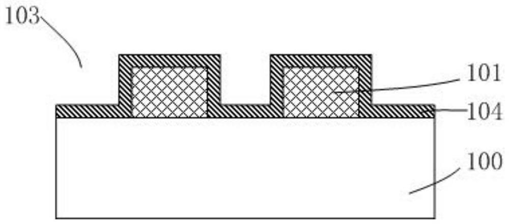
[0030] refer to image 3 A sidewall material layer 104 is formed on the bottom and sidewall surfaces of the ...
PUM
 Abstract
Description
Claims
Application Information