Semiconductor manufacturing scheduling method and system and computer readable storage medium

A semiconductor and random sequence technology, applied in the field of semiconductor manufacturing scheduling methods, systems, and computer-readable storage media, can solve problems such as large amount of calculations and time-consuming solutions, so as to reduce production costs, rationally allocate production capacity, and improve The effect of resource utilization

Pending Publication Date: 2022-05-10
埃克斯工业有限公司
View PDF0 Cites 1 Cited by
  • Summary
  • Abstract
  • Description
  • Claims
  • Application Information

AI Technical Summary

Problems solved by technology

[0003] At present, there is an existing semiconductor production scheduling method that uses evolutionary laws to construct intelligent optimization algorithms such as genetic algorithms for querying, but this method needs to construct sequence populations and perform optimization iterations in the populations, and requires Each individual is calculated separately. When the population is larger, the amount of calculation is also greater, resulting in a large amount of time for a solution.

Method used


Image

  • Semiconductor manufacturing scheduling method and system and computer readable storage medium
  • Semiconductor manufacturing scheduling method and system and computer readable storage medium
  • Semiconductor manufacturing scheduling method and system and computer readable storage medium

Examples


Embodiment Construction

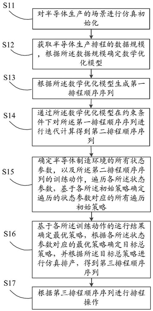
[0049] This embodiment takes a semiconductor manufacturing scheduling method and system as an example, and the present invention will be described in detail below in conjunction with specific embodiments and accompanying drawings.

[0050] A semiconductor manufacturing production scheduling method provided by an embodiment of the present invention includes the following steps:

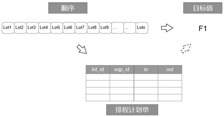
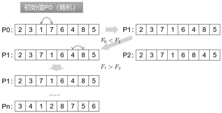
[0051] Obtaining the data scale of semiconductor manufacturing scheduling, determining a mathematical optimization model according to the data scale; generating a first scheduling order sequence according to the mathematical optimization model, and using the mathematical optimization model to perform the first scheduling under constraints Performing iterative calculation on the sequence sequence to obtain the second schedule sequence sequence, the second schedule sequence sequence is the schedule sequence sequence with the largest adaptive value under the constraints, and the constraints include the maxim...


PUM


Abstract

The invention discloses a semiconductor manufacturing scheduling method and system and a computer readable storage medium. The method comprises the following steps: determining a mathematical optimization model according to a data scale; generating a first scheduling sequence according to the mathematical optimization model, and performing iterative calculation on the first scheduling sequence through the mathematical optimization model under a constraint condition to obtain a second scheduling sequence; determining an optimal strategy based on an operation result of each training action, determining a target total strategy according to the optimal strategy corresponding to each state parameter, and performing simulation scheduling according to the target total strategy to obtain a third scheduling sequence; and performing scheduling operation according to the third scheduling sequence. According to the method, rapid target optimization of semiconductor manufacturing scheduling is realized, the production capacity is effectively and reasonably distributed, the resource utilization rate is improved, and the production cost is reduced.

Description

technical field [0001] The present invention relates to the technical field of semiconductor manufacturing, in particular to a semiconductor manufacturing scheduling method, system and computer-readable storage medium. Background technique [0002] Semiconductor manufacturing is one of the complex industrial manufacturing chains, which usually includes four production stages: wafer fabrication, wafer sorting, packaging and product testing. Among them, wafer fabrication is a complex work, with hundreds of process steps required for the manufacture of machines and silicon wafers. A small part of the products exist in hundreds of processes in the factory, therefore, it is necessary to create complex capacity allocation and job scheduling problems, that is, scheduling problems are closely concerned issues in semiconductor manufacturing. Scheduling problem generally means that n workpieces are processed in a pipeline on m machines. Each workpiece takes different time to run on e...

Claims


Application Information

Patent Timeline
Patent Type & Authority Applications(China)
IPC IPC(8): G06Q10/06G06Q50/04G06N3/12
CPCG06Q10/06316G06Q50/04G06N3/126Y02P90/30
Inventor 肖俊河李杰刘斌郭宇翔傅慧初
Owner 埃克斯工业有限公司
Why Eureka
Try Eureka