
Formation method of semiconductor structure

A semiconductor and sidewall structure technology, which is applied in semiconductor devices, semiconductor/solid-state device manufacturing, electrical components, etc., can solve the problems of threshold voltage drift, poor uniformity of contact holes, inconsistent metal gate resistance, etc., and achieve high uniformity , high uniformity, good effect of high consistency

Pending Publication Date: 2022-05-13
SEMICON MFG INT (SHANGHAI) CORP +1
View PDF0 Cites 0 Cited by
  • Summary
  • Abstract
  • Description
  • Claims
  • Application Information

AI Technical Summary

Problems solved by technology

[0003] However, it is difficult to control the height of the existing metal gates, and the height uniformity of the metal gates is poor, which easily leads to inconsistent resistance of different metal gates and threshold voltage drift.
In addition, in the self-aligned contact hole formation process, the filling material in the planarized contact hole usually stops on the protective layer on the metal gate, and the non-uniform metal gate will easily lead to poor uniformity of the self-aligned contact hole. The performance of the resulting semiconductor device is poor
[0004] Therefore, the performance of existing semiconductor devices is poor

Method used


Image

  • Formation method of semiconductor structure
  • Formation method of semiconductor structure
  • Formation method of semiconductor structure

Examples


Embodiment Construction

[0037] It should be noted that the "surface" and "upper" in this specification are used to describe the relative positional relationship in space, and are not limited to direct contact.

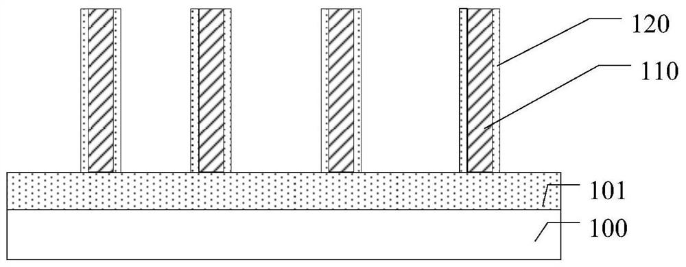
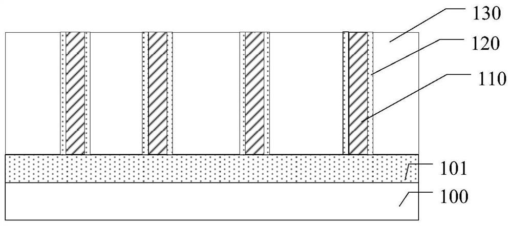
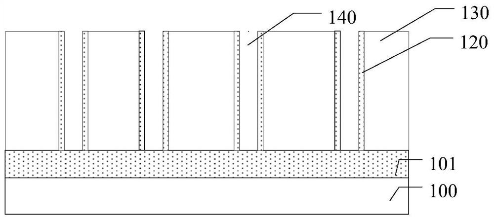
[0038] Firstly, the reason for the poor performance of the existing semiconductor structure will be described in detail with reference to the accompanying drawings. Figure 1 to Figure 4 It is a structural schematic diagram of each step of a method for forming a conventional semiconductor structure.

[0039] Please refer to figure 1 , providing a base, the base includes a substrate 100, a fin 101 located on the surface of the substrate 100, and an isolation layer (not shown in the figure), the isolation layer covers part of the surface of the side wall of the fin 101, and the base has The dummy gate structure 110 across the fin portion 101 has sidewall structures 120 on both sides of the dummy gate structure 110 .

[0040] Please refer to figure 2 , forming a dielectric layer 130 on the s...


PUM

PropertyMeasurementUnit
relative permittivityaaaaaaaaaa

Abstract

A method for forming a semiconductor structure comprises the following steps: providing a substrate which is provided with a plurality of dummy gate structures; forming an initial dielectric layer on the substrate, wherein the initial dielectric layer is located on the surface of the side wall of the dummy gate structure; the initial dielectric layer is etched to form a dielectric layer, and the top surface of the dielectric layer is lower than the top surface of the dummy gate structure; removing the dummy gate structure, and forming a first opening in the dielectric layer; forming a gate structure material film in the first opening and on the surface of the dielectric layer; and planarizing the gate structure material film until the top surface of the dielectric layer is exposed to form a gate structure. The method is beneficial to improving the performance of the formed semiconductor structure.

Description

technical field [0001] The invention relates to the technical field of semiconductor manufacturing, in particular to a method for forming a semiconductor structure. Background technique [0002] With the decreasing size of semiconductor devices, more and more device units are integrated per unit area, the density of devices is gradually increasing, and the size between devices is decreasing, which also increases the difficulty of manufacturing. As the critical dimension (CD) of integrated circuits shrinks, a "gate-last process" is usually used to form the metal gate. The gate-last process requires forming a gate opening in the dielectric layer and filling the gate opening with a gate material. [0003] However, it is difficult to control the height of the existing metal gates, and the height uniformity of the metal gates is poor, which easily leads to inconsistent resistances of different metal gates and threshold voltage drift. In addition, in the self-aligned contact hol...

Claims


Application Information

Patent Timeline
Patent Type & Authority Applications(China)
IPC IPC(8): H01L21/336H01L29/78
CPCH01L29/66795H01L29/7851H01L29/66545
Inventor 苏博姜长城王文泰
Owner SEMICON MFG INT (SHANGHAI) CORP
Learn More