

Semiconductor packaging mold
A semiconductor and mold technology, applied in the field of semiconductor packaging molds, can solve the problems of cumbersome operation, low degree of automation of semiconductor packaging, and reduced efficiency of semiconductor packaging, so as to achieve the effects of increasing automation, facilitating replacement, and improving packaging efficiency
- Summary
- Abstract
- Description
- Claims
- Application Information
AI Technical Summary
Problems solved by technology
Method used
Image

Examples
Embodiment 1
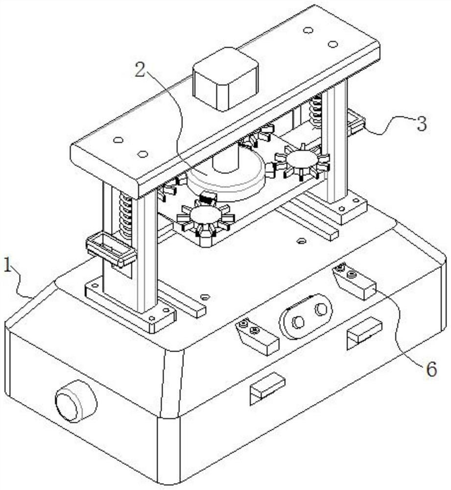
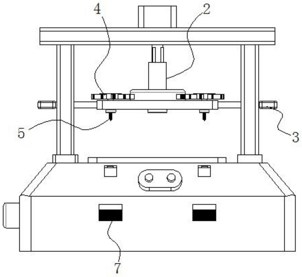
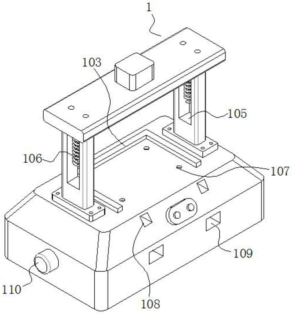
[0035] see Figure 1-13 , the present invention is a semiconductor packaging mold, including a drive mechanism 1, the drive mechanism 1 includes a mounting base 101 and a concave support frame 102 fixed on the top of the mounting base 101, the top of the mounting base 101 is fixed with a limit ring 103, through the limit The arrangement of the ring 103 enables the packaging box containing the semiconductor material to be confined inside the limiting ring 103, thereby preventing the position of the packaging box from moving during the packaging process;
[0036] A No. 1 stepping motor 104 is installed on the top of the concave support frame 102 , a clamping piece is fixed at the lower end of the output shaft of the No. 1 stepping motor 104 , a transmission component 2 is sleeved outside the clamping piece, and a package component 3 is rotatably connected to the bottom of the transmission component 2 . The four corners of the surface of the package assembly 3 are rotatably conne...
Embodiment 2
[0051] On the basis of Embodiment 1, according to the use of screws 5 in different types of grooves on the packaging box, the corresponding type of screw screw assembly 4 can be replaced to meet the needs of tightening and fixing the screws 5 on the packaging box.
PUM
 Abstract
Description
Claims
Application Information