Unlock instant, AI-driven research and patent intelligence for your innovation.

Display substrate, preparation method thereof and display device

A technology for displaying substrates and extension directions, applied in identification devices, semiconductor/solid-state device manufacturing, instruments, etc., can solve problems such as increasing the thickness of display screens, achieve the effects of reducing the number of film layers, meeting bending requirements, and reducing overall thickness

Pending Publication Date: 2022-05-27
BOE TECH GRP CO LTD +1
View PDF0 Cites 0 Cited by
  • Summary
  • Abstract
  • Description
  • Claims
  • Application Information

AI Technical Summary

Problems solved by technology

Increasing the film layer will inevitably increase the thickness of the display, and the thicker the thickness, the more risks and difficulties there will be in bending the flexible display

Method used


Image

  • Display substrate, preparation method thereof and display device
  • Display substrate, preparation method thereof and display device
  • Display substrate, preparation method thereof and display device

Examples


Embodiment Construction

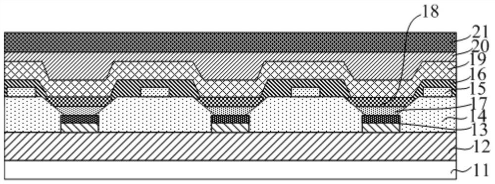
[0037] The present invention will be further described in detail below in conjunction with the accompanying drawings and embodiments. It should be understood that the specific embodiments described herein are only used to explain the related invention, but not to limit the invention. In addition, it should be noted that, for the convenience of description, only the parts related to the invention are shown in the drawings.

[0038] It should be noted that the embodiments of the present invention and the features of the embodiments may be combined with each other under the condition of no conflict. The present invention will be described in detail below with reference to the accompanying drawings and in conjunction with the embodiments.

[0039] In the description of the present invention, it should be understood that the terms "center", "longitudinal", "lateral", "length", "width", "thickness", "upper", "lower", "front", " Back, Left, Right, Vertical, Horizontal, Top, Bottom,...


PUM


Abstract

The invention discloses a display substrate, a preparation method thereof and a display device. The display substrate comprises a substrate and a first electrode located on one side of the substrate. The pixel defining layer is located on the side, away from the substrate, of the first electrode, and the pixel defining layer is provided with an opening area exposing the first electrode and an edge area covering the first electrode; the second electrode is located on the side, away from the substrate, of the pixel defining layer and located in the non-opening area of the pixel defining layer; the insulating layer is located in the non-opening area of the pixel defining layer and covers the second electrode; the light-emitting layer is located on the side, away from the substrate, of the first electrode and located in the opening area of the pixel defining layer; the cathode layer is located on the side, away from the substrate, of the insulating layer and covers the insulating layer and the light-emitting layer, the extending direction of the second electrode intersects with the extending direction of the cathode layer, and a touch capacitor is formed between the second electrode and the cathode layer. The touch structure is realized in the display substrate, so that the overall thickness of a display screen can be reduced, and the bending requirement of a flexible screen can be better met.

Description

technical field [0001] The present invention generally relates to the field of display technology, and specifically relates to a display substrate, a preparation method thereof, and a display device. Background technique [0002] There are usually two ways to realize the touch function of traditional OLED (Organic Light-Emitting Diode) display with touch function. One way is to attach a layer of cover plate with metal traces to realize The touch function is widely known as OGS (One Glass Solution, monolithic touch screen) technology in the industry; another way is to directly fabricate metal traces on the thin film encapsulation layer (Thin-Film Encapsulation, TFE) to realize the touch function. The industry is widely known as On-Cell technology, for example: FMLOC (Flexible Multi-Layer On Cell, flexible multi-layer structure) technology. [0003] However, whether it is OGS technology or On-Cell technology, many layers or functional layers need to be provided to realize the...

Claims


Application Information

Patent Timeline
Patent Type & Authority Applications(China)
IPC IPC(8): H01L27/32H01L51/52H01L51/56G09F9/30G09F9/33
CPCG09F9/301G09F9/33H10K59/40H10K50/82H10K71/00Y02E10/549
Inventor 赖韦霖陈思毫
Owner BOE TECH GRP CO LTD