Electroluminescent display device
A technology of electroluminescent display and light-emitting layer, which is applied in the direction of circuits, electrical components, electric solid-state devices, etc., and can solve the problems of increasing manufacturing costs
- Summary
- Abstract
- Description
- Claims
- Application Information
AI Technical Summary
Problems solved by technology
Method used
Image


Examples
no. 1 approach -
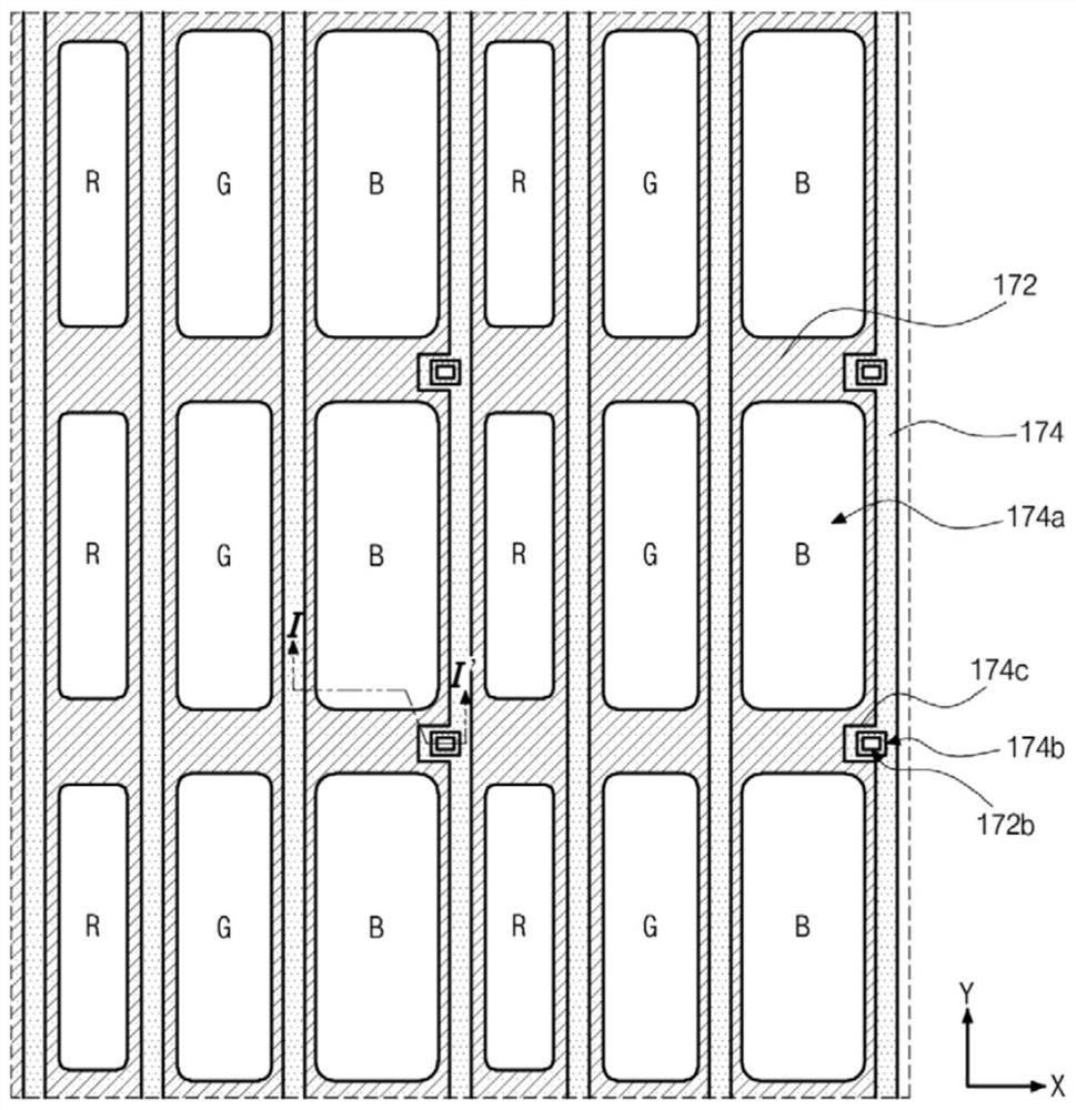
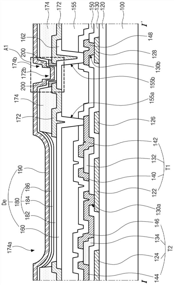
[0059] image 3 is a schematic cross-sectional view of an electroluminescent display device according to a first embodiment of the present disclosure. image 3 corresponds to figure 2 line I-I', and shows a pixel area.
[0060] exist image 3 Among them, the buffer layer 120 is formed on substantially the entire surface of the substrate 100 . The substrate 100 may be a glass substrate or a plastic substrate. For example, polyimide may be used for the plastic substrate, but is not limited thereto.
[0061] The buffer layer 120 may be made of, for example, silicon oxide (SiO 2 ) or an inorganic insulating material of silicon nitride (SiNx), and may be formed as a single layer or multiple layers.
[0062] A first gate electrode 122 , a second gate electrode 124 , a capacitor electrode 126 , and a first auxiliary electrode 128 of a conductive material such as metal are formed on the buffer layer 120 .
[0063] The first gate electrode 122 , the second gate electrode 124 , ...
no. 2 approach -
[0189] Figure 7 and Figure 8 corresponding to image 3 A schematic enlarged plan view and a schematic enlarged cross-sectional view of the area A1 of . Figure 7 is a top view showing the planar structure of the auxiliary pattern in the electroluminescence display device according to the second embodiment of the present disclosure, Figure 8 is corresponding to Figure 7 A cross-sectional view of the line III-III'. The electroluminescent display device according to the second embodiment of the present disclosure has substantially the same configuration as the electroluminescent display device of the first embodiment except for the auxiliary patterns. The same parts as those of the first embodiment are denoted by the same reference numerals, and the description of the same parts will be shortened or omitted.
[0190] exist Figure 7 and Figure 8 , the second charge auxiliary layer 186 is formed between the connection pattern 162 and the second electrode 190 , correspo...
no. 3 approach -
[0202] Figure 9 and Figure 10 corresponding to image 3 A schematic enlarged plan view and a schematic enlarged cross-sectional view of the area A1 of . Figure 9 is a top view showing the planar structure of the auxiliary pattern in the electroluminescence display device according to the second embodiment of the present disclosure, Figure 10 is corresponding to Figure 9 A cross-sectional view of the line IV-IV'. The electroluminescent display device according to the third embodiment of the present disclosure has substantially the same configuration as the electroluminescent display device of the first embodiment except for the auxiliary patterns. The same parts as those of the first embodiment are denoted by the same reference numerals, and the description of the same parts will be shortened or omitted.
[0203] exist Figure 9 and Figure 10 , the second charge auxiliary layer 186 is formed between the connection pattern 162 and the second electrode 190 , correspo...
PUM
| Property | Measurement | Unit |
|---|---|---|
| angle | aaaaa | aaaaa |
| length | aaaaa | aaaaa |
Abstract
Description
Claims
Application Information
PatSnap Eureka turns technology decisions into work you can execute. Powered by our Innovation Knowledge Graph, it runs expert workflows across engineering, life sciences, materials and intellectual property. Get your review-ready output in minutes.


