Scanning path optimization method, application and semiconductor material surface detection method

A scanning path and optimization method technology, which is applied in semiconductor/solid-state device testing/measurement, material analysis, material analysis through optical means, etc., can solve the problem of increasing scanning imaging time and scanning space, lack of distribution planning, and low detection efficiency and other problems, to achieve the effect of reducing image scanning, reducing the number, and accurate detection results

Active Publication Date: 2022-06-07
WUHAN JINGLI ELECTRONICS TECH +1
View PDF14 Cites 0 Cited by
  • Summary
  • Abstract
  • Description
  • Claims
  • Application Information

AI Technical Summary

Problems solved by technology

[0009] Therefore, although the existing technology also considers saving the number of pictures as much as possible, it does not obtain an optimal imaging field of view. rect N The distribution planning increases the scanning imaging time and scanning space, and the detection efficiency is low and cumbersome

Method used


Image

  • Scanning path optimization method, application and semiconductor material surface detection method
  • Scanning path optimization method, application and semiconductor material surface detection method
  • Scanning path optimization method, application and semiconductor material surface detection method

Examples


Embodiment Construction

[0035]In order to make the objectives, technical solutions and advantages of the present invention clearer, the present invention will be further described in detail below with reference to the accompanying drawings and embodiments. It should be understood that the specific embodiments described herein are only used to explain the present invention, but not to limit the present invention. In addition, the technical features involved in the various embodiments of the present invention described below can be combined with each other as long as they do not conflict with each other.

[0036] Those skilled in the art can easily understand that the above are only preferred embodiments of the present invention, and are not intended to limit the present invention. Any modifications, equivalent replacements and improvements made within the spirit and principles of the present invention, etc., All should be included within the protection scope of the present invention.
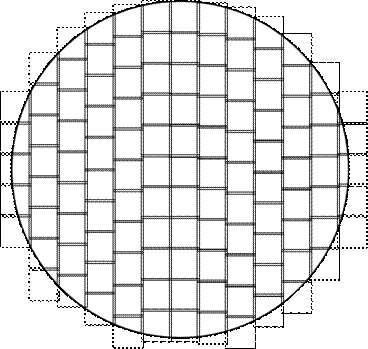
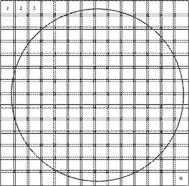
[0037] It shou...


PUM


Abstract

The invention provides an optimization method and application of a scanning path and a detection method of a semiconductor material surface, and belongs to the technical field of semiconductor surface detection.According to the optimization method of the scanning path, limiting conditions of a to-be-scanned area, a scanning imaging view field and an overlapping area serve as constant parameters; establishing an inequality model by taking the scanning number and the actual overlapping area as parameters needing to be optimized; and integer solution is carried out on the inequality model to obtain a plan of a scanning path in which the number of scanned pictures is minimum and the overlapping area of two adjacent imaging view fields is maximum under the same condition. According to the method, any hardware change is not needed, the scanning time of the whole wafer can be effectively saved, and the processing number and the storage capacity of imaging view images are reduced.

Description

technical field [0001] The invention belongs to the technical field of semiconductor material detection, and in particular relates to an optimization method and application of a scanning path and a detection method for the surface of a semiconductor material. Background technique [0002] Semiconductor materials are generally used in the process of manufacturing semiconductor wafers, and thus, the production capacity of semiconductor materials has a very large impact on the entire integrated circuit industry. At present, the main semiconductor material is wafer, and more than 90% of electronic devices on the market are manufactured based on wafers. Since the surface of the semiconductor material directly affects the processing performance of the device, it is not allowed to have any defects on the surface; in the industrial production process, the detection system needs to perform real-time detection, and there is a problem of high detection difficulty. The existing technolo...

Claims


Application Information

Patent Timeline
Patent Type & Authority Applications(China)
IPC IPC(8): G01N21/95H01L21/66
CPCG01N21/9501H01L22/12H01L22/20
Inventor 张胜森刘荣华
Owner WUHAN JINGLI ELECTRONICS TECH
Why Eureka
Try Eureka