Pixel driving circuit, driving method and display device

A pixel driving circuit and driving voltage technology, which is applied in the field of driving methods, display devices, and pixel driving circuits, can solve problems such as the inability to eliminate parasitic charges in compensation circuits, and achieve the effect of eliminating parasitic charges and avoiding influence

Pending Publication Date: 2022-06-17
HKC CORP LTD
View PDF9 Cites 0 Cited by
  • Summary
  • Abstract
  • Description
  • Claims
  • Application Information

AI Technical Summary

Problems solved by technology

[0003] The present application provides a pixel driving circuit, a driving method and a display device, aiming to solve the problem that the parasitic charge in the compensation circuit cannot be eliminated in the exemplary technology

Method used


Image

  • Pixel driving circuit, driving method and display device
  • Pixel driving circuit, driving method and display device
  • Pixel driving circuit, driving method and display device

Examples


Embodiment 1

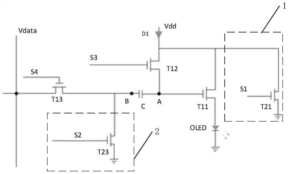
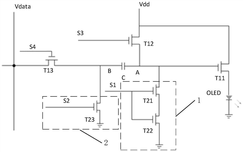
[0036] figure 1 is a schematic structural diagram of a pixel driving circuit provided by the embodiment of the present application, such as figure 1 As shown, it specifically includes: a compensation capacitor unit C, the first terminal A of the compensation capacitor unit C is coupled to the driving voltage terminal Vdd, and the second terminal B is coupled to the data voltage terminal Vdata; The control end of a switch unit T11 is coupled to the first end A of the compensation capacitor unit C, the input end is coupled to the driving voltage end Vdd, and the output end is coupled to a light-emitting device; the first discharge module 1, in the first stage, The driving voltage written in the first terminal A of the compensation capacitor unit C is reduced to the first set threshold; and the second discharge module 2 reduces the data voltage written in the second terminal B of the compensation capacitor unit C in the second stage to the second set threshold; wherein in the se...

Embodiment 2

[0067] like Figure 5 As shown, a display device 20 in an embodiment of the present application includes a display panel and a pixel driving circuit 22 as in Embodiment 1, the display panel includes a plurality of pixel units, and each pixel unit includes a plurality of light-emitting devices 23, Each light-emitting device is coupled to the output end of the first switch unit T11 of the pixel driving circuit in Embodiment 1 of the present application through a wire 21 .

[0068] During specific implementation, the display device provided by the embodiment of the present invention may be any product or component with display function, such as a mobile phone, a tablet computer, a television, a monitor, a notebook computer, a digital photo frame, and a navigator.

[0069] It can be understood that the display device in this application discharges the compensation capacitor unit C at different stages through two discharge modules, and further provides a discharge channel for the com...

Embodiment 3

[0071] The embodiment of the present application further provides a driving method of a display device, the driving method is performed by using the pixel driving circuit in the above-mentioned embodiment 1, and specifically includes:

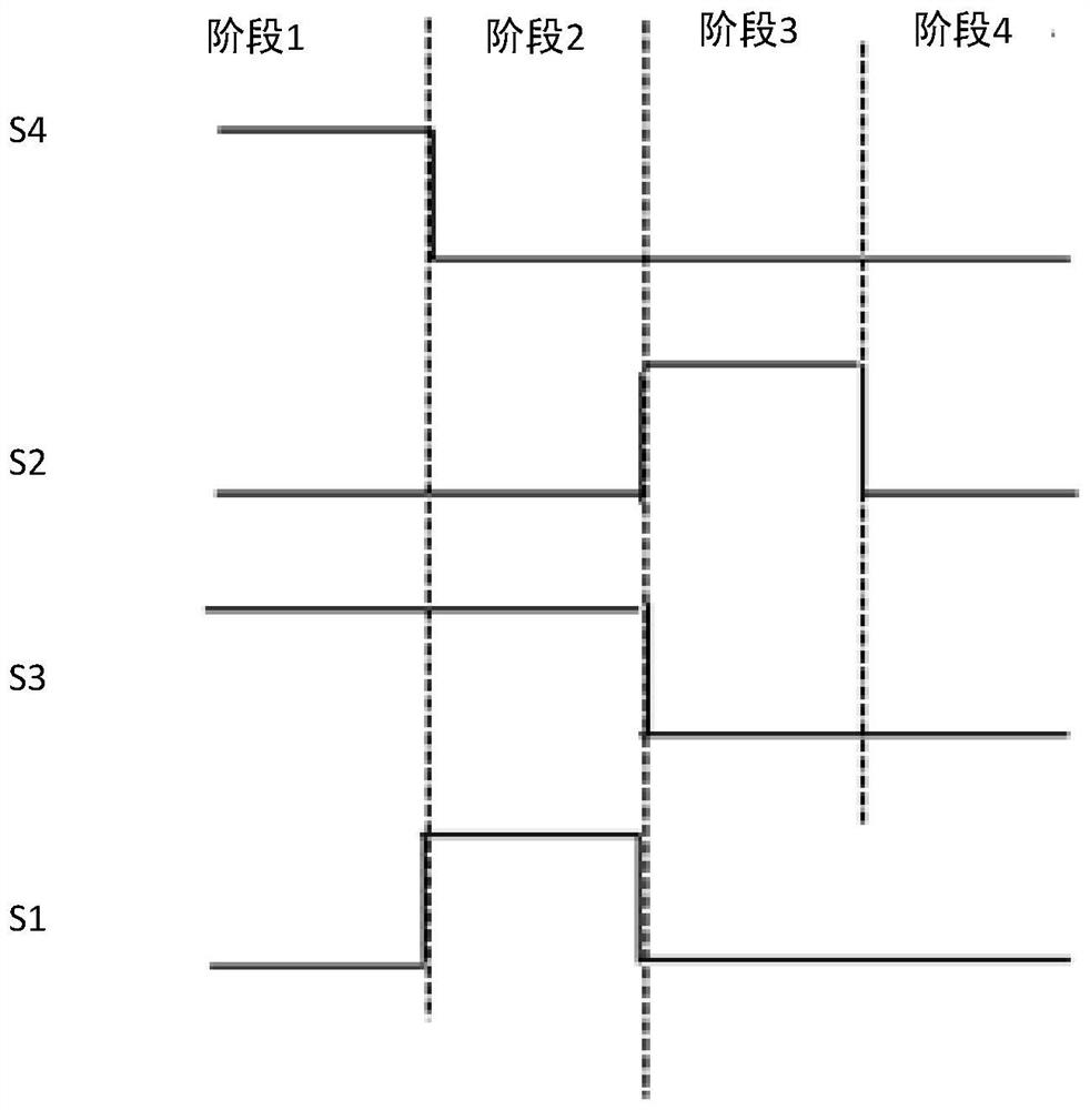
[0072] S1: write a driving voltage to the first end A of the compensation capacitor unit C, and write a data voltage to the second end B;

[0073] S2: in the first stage, reducing the driving voltage written in the first terminal A of the compensation capacitor unit C to a first set threshold;

[0074] S3: In the second stage, the data voltage written in the second terminal B of the compensation capacitor unit C is reduced to a second set threshold, and the first discharge module and the first terminal of the compensation capacitor unit C are disconnected A, so that the voltage of the first terminal A of the compensation capacitor unit C jumps to a target voltage, and the target voltage is greater than the threshold voltage of the first switch ...


PUM


Abstract

According to the pixel driving circuit, the driving method and the display device provided by the invention, the current passing through the organic light-emitting diode can be irrelevant to the negative electrode of the power supply and the threshold voltage of each thin film transistor, so that the display can be homogenized; in addition, two discharge modules discharge the compensation capacitor unit at different stages, so that a discharge channel is provided for the compensation capacitor unit at each stage, parasitic charges in the circuit can be eliminated, and on the premise that pixel driving compensation can be carried out, the pixel driving compensation efficiency is improved. Parasitic charges generated in the operation process of the whole circuit are efficiently eliminated, and therefore the influence of the parasitic charges on driving of the organic light-emitting device is avoided.

Description

technical field [0001] The present application relates to the field of display technology, and in particular, to a pixel driving circuit, a driving method and a display device. Background technique [0002] With the development of the field of liquid crystal display, the advantages of organic light-emitting display (OLED) display technology, such as self-luminescence, lightness and thinness, have gradually been widely used in TV, mobile phones, notebooks and other products. Because OLED belongs to current Drive, when the threshold voltage Vth of the thin film transistor (Thin Film Transistor, TFT) shifts, the current drive of the OLED will not be stable and change, which will cause uneven brightness. At present, the current compensation is performed by the drive compensation circuit. However, there is a problem that the parasitic charge of the circuit cannot be eliminated. SUMMARY OF THE INVENTION [0003] The present application provides a pixel driving circuit, a drivin...

Claims


Application Information

Patent Timeline
IPC IPC(8): G09G3/3225
CPCG09G3/3225G09G2320/0233G09G2320/02
Inventor 周仁杰郑浩旋
Owner HKC CORP LTD
Why Eureka
Try Eureka