Display panel and mobile terminal

A display panel and branch electrode technology, which is applied in the direction of instruments, nonlinear optics, optics, etc., can solve the problems of panel vertical crosstalk and affect the panel display effect, and achieve the effect of increasing the overlapping area, improving the display effect, and preventing vertical crosstalk

Pending Publication Date: 2022-06-24
TCL CHINA STAR OPTOELECTRONICS TECH CO LTD
View PDF7 Cites 0 Cited by
  • Summary
  • Abstract
  • Description
  • Claims
  • Application Information

AI Technical Summary

Problems solved by technology

However, due to the unavoidable layering and cross-line structure between metals in the panel design, there will inevitably be some parasitic capacitance, such as the parasitic capacitance between the data line and the pixel electrode. The existence of parasitic capacitance will affect the display of the panel. Effect
When the parasitic capacitance between the data line and the pixel electrode is too large, it will cause undesirable problems such as vertical crosstalk on the panel

Method used


Image

  • Display panel and mobile terminal
  • Display panel and mobile terminal
  • Display panel and mobile terminal

Examples


Embodiment 1

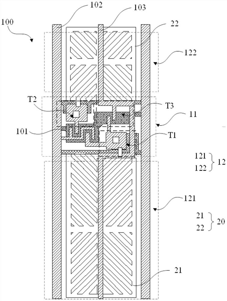
[0036] like figure 1 As shown, it is a schematic diagram of the pixel structure of the display panel 100 provided by the first embodiment of the present application; wherein, the display panel 100 includes a plurality of sub-pixels arranged in an array, and each sub-pixel is an eight-domain 2110 pixel structure.

[0037] Wherein, the display panel 100 further includes a plurality of scan lines 101 and a plurality of data lines 102 , and the sub-pixels are formed in the intersection regions of the plurality of the scan lines 101 and the plurality of the data lines 102 .

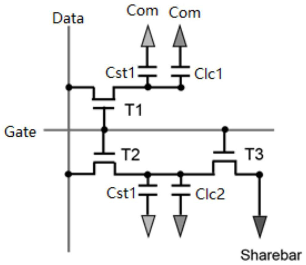
[0038] like figure 2 shown is a schematic diagram of an equivalent circuit of the pixel structure in the display panel 100 provided by the first embodiment of the present application; combined with figure 1 as well as figure 2 It can be seen that each of the sub-pixels includes a thin film transistor region 11 and a pixel electrode region 12, and the pixel electrode region 12 includes a first sub-pixel ele...

Embodiment 2

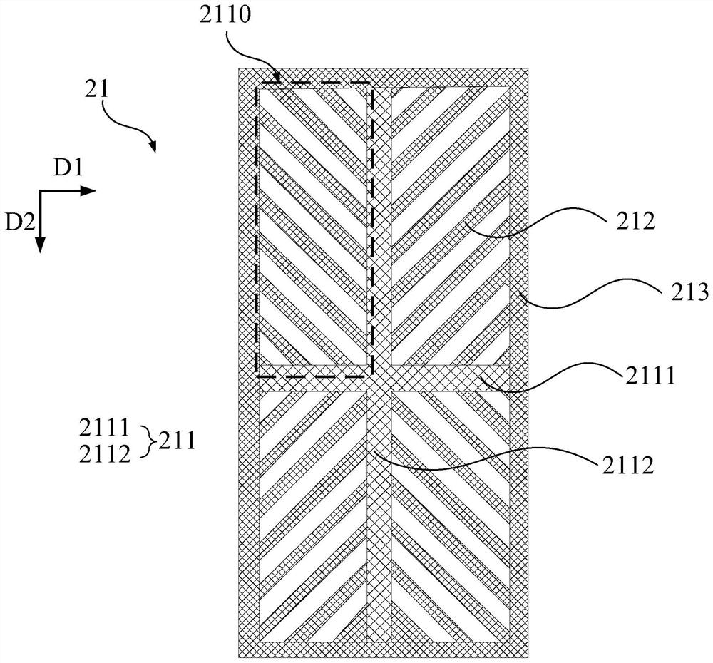
[0087] like Figure 4 shown in the figure is a schematic structural diagram of the first sub-pixel electrode 20 in the display panel 100 provided by the second embodiment of the present application; wherein, the structure of the display panel 100 in the second embodiment of the present application is the same as that of the display panel in the first embodiment of the present application. 100 has the same or similar structure, the only difference is that, in each of the domains 2110, the branch electrodes 212 extend from the main electrode 211 in different directions, and two adjacent branch electrodes 212 are far away from each other. A plurality of first openings 2121 are formed at one end of the trunk electrode 211 (ie, the pixel electrode 20 is not provided with the first enclosing frame electrode 213 ).

[0088] Compared with the display panel 100 provided in the first embodiment of the present application, the display panel 100 provided by the second embodiment of the pr...

Embodiment 3

[0091] like Figure 5 shown in the figure is a schematic structural diagram of the first sub-pixel electrode 20 in the display panel 100 provided by the third embodiment of the present application; wherein, the structure of the display panel 100 in the third embodiment of the present application is the same as that of the display panel 100 in the first embodiment of the present application. The structure is the same or similar, except that the main electrode 211 includes a third sub-electrode 2113 arranged along the first direction D1 and a peripheral electrode 2114 arranged around a plurality of the branch electrodes 212. The third sub-electrode 2114 The electrode 2113 divides the sub-pixel into two of the domains 2110;

[0092] The branch electrode 212 includes a plurality of first sub-branch electrodes 212 and a plurality of second sub-branch electrodes 212, one end of the first sub-branch electrode 212 is electrically connected to the third sub-electrode 2113, and the The...


PUM


Abstract

The embodiment of the invention provides a display panel and a mobile terminal. The display panel comprises a plurality of sub-pixels, each sub-pixel comprises a pixel electrode and a common electrode arranged on the different layer of the pixel electrode, and in the top view direction of the display panel, the orthographic projection of the common electrode on the pixel electrode coincides with the pixel electrode; according to the display panel, the orthographic projection, on the pixel electrode, of the common electrode in each sub-pixel coincides with the pixel electrode, so that the overlapping area of the common electrode and the pixel electrode in the direction perpendicular to the display panel is increased, and then the load capacitance of the pixel electrode is increased; therefore, stray capacitance generated between the data lines and the pixel electrodes is further reduced, the vertical crosstalk phenomenon of a picture of the display panel is prevented, and the display effect of the display panel is further improved.

Description

technical field [0001] The present application relates to the field of display technology, and in particular, to a display panel and a mobile terminal. Background technique [0002] With the continuous development of liquid crystal display technology, liquid crystal display devices such as liquid crystal display panels (Light Emitting Diode Panel) have been widely used as display components in electronic products such as mobile phones, digital cameras, and personal digital assistants. [0003] At present, thin film transistors (Thin Film Transistors) are widely used in liquid crystal display panels. However, due to the inevitable existence of stacking and cross-line structures between metals in panel design, there will inevitably be some parasitic capacitances, such as parasitic capacitances between data lines and pixel electrodes. The existence of parasitic capacitances will affect the display of the panel. Effect. When the parasitic capacitance between the data line and ...

Claims


Application Information

Patent Timeline
Patent Type & Authority Applications(China)
IPC IPC(8): G02F1/1343
CPCG02F1/134309
Inventor 陈艳玲
Owner TCL CHINA STAR OPTOELECTRONICS TECH CO LTD
Why Eureka
Try Eureka