Pixel circuit, pixel driving method and display device

A technology of pixel circuits and driving transistors, applied in static indicators, instruments, etc., can solve the problems of low luminous efficiency of OLED displays, and achieve the effects of enhanced display screen effect, long service life and high brightness uniformity

Active Publication Date: 2022-06-24
CHANGSHA HKC OPTOELECTRONICS CO LTD +1
View PDF8 Cites 1 Cited by
  • Summary
  • Abstract
  • Description
  • Claims
  • Application Information

AI Technical Summary

Problems solved by technology

[0002] At present, in the OLED display panel, the pixel circuit often uses a 2T1C circuit, that is, it includes two transistors and a capacitor, and t

Method used


Image

  • Pixel circuit, pixel driving method and display device
  • Pixel circuit, pixel driving method and display device
  • Pixel circuit, pixel driving method and display device

Examples


Embodiment 1

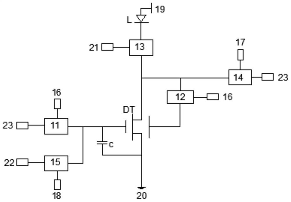
[0065] Embodiments of the present disclosure provide a pixel circuit for implementing pixel compensation. like figure 1 As shown, the pixel circuit may include a light-emitting element L, a capacitive structure C, a dual-gate driving transistor DT, a first switching element 11, a second switching element 12, a third switching element 13, a fourth switching element 14 and a fifth switching element 15.

[0066] It should be understood that the light-emitting element L and the capacitor structure C both have a first terminal and a second terminal, and the dual-gate driving transistor DT has a first control terminal and a second control terminal in addition to the first terminal and the second terminal; The relationship between the first to fifth switching elements 15 and the light-emitting element L, the capacitance structure C, and the dual-gate drive transistor DT is as follows.

[0067] The first switching element 11 can be used to respond to the first scan signal S n-1 , s...

Embodiment 2

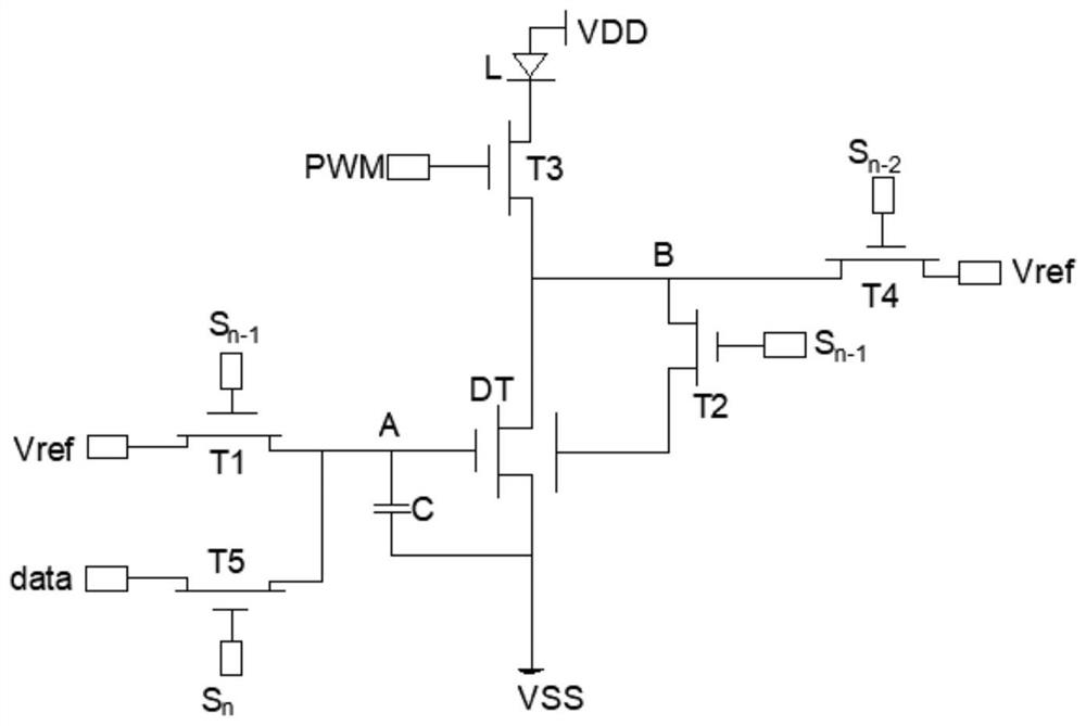
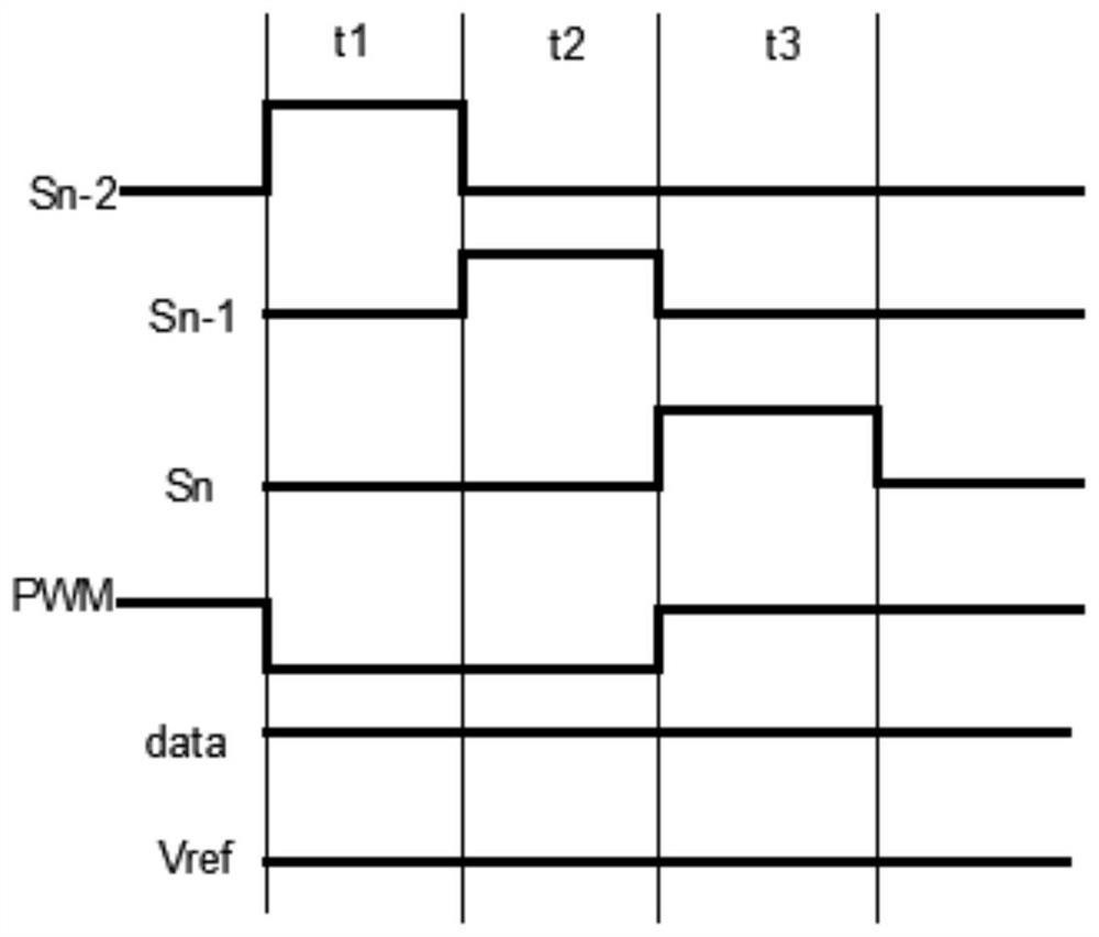
[0096] Based on the pixel circuit mentioned in the first embodiment, the second embodiment of the present disclosure further provides a pixel driving method, which combines figure 2 , image 3 and Figure 4 , the pixel driving method may include:

[0097] Step S300, in the reset stage, use the second scan signal S n-2 The fourth switching element 14 is turned on, and at the same time, the first scan signal S is used n-1 , the third scan signal S n and the pulse width modulation signal PWM to turn off the first switching element 11 , the second switching element 12 , the fifth switching element 15 and the third switching element 13 ;

[0098] Step S310, in the compensation stage, use the first scan signal S n-1 The first switching element 11 and the second switching element 12 are turned on, and at the same time, the second scanning signal S is used n-2 , the third scan signal S n and the pulse width modulation signal PWM to turn off the fourth switching element 14, the...

Embodiment 3

[0114] Based on the content of the foregoing first embodiment, the third embodiment further provides a display device, which may be an OLED display device. The display device may include a substrate and a plurality of pixel groups, and the substrate may be made of glass, but not limited thereto, and may also be polyimide (PI) depending on the specific situation.

[0115] The substrate may have a display area, and a plurality of pixel groups are located in the display area. The pixel group may include a pixel circuit. For details, refer to the content of the first embodiment, which will not be repeated here. combine figure 1 and figure 2 shown, this pixel group may also include:

[0116] The first scan signal line 16 can be electrically connected to the first switch element 11 and the second switch element 12 for providing the first scan signal Sn-1;

[0117] The second scan signal line 17 can be electrically connected to the fourth switch element 14 for providing the seco...


PUM


Abstract

The invention relates to a pixel circuit, a pixel driving method and a display device. The pixel circuit comprises a light-emitting element, a capacitor structure, a double-gate type driving transistor and first to fifth switch elements, and the first switch element is used for responding to a first scanning signal so as to apply a reference signal to a first control end of the double-gate type driving transistor; the second switch element is used for responding to the first scanning signal, so that a second control end of the double-gate type driving transistor is connected with a first end of the double-gate type driving transistor and a first end of the fourth switch element respectively; the third switch element is used for responding to a pulse width modulation signal so as to connect the first end of the light-emitting element with the first end of the double-gate driving transistor; the fourth switch element is used for responding to a second scanning signal so as to apply the reference signal to the first end of the double-gate type driving transistor. According to the scheme, the display uniformity can be improved.

Description

technical field [0001] The present application belongs to the field of display technology, and in particular relates to a pixel circuit, a pixel driving method and a display device. Background technique [0002] At present, in the OLED display panel, the pixel circuit often adopts a 2T1C circuit, that is, it includes two transistors and a capacitor, and the two transistors are a switching transistor and a driving transistor respectively, but this will lead to a low luminous efficiency of the OLED display. SUMMARY OF THE INVENTION [0003] The purpose of the present disclosure is to provide a pixel circuit, a pixel driving method and a display device, which can adopt the form of top emission, so that the emission efficiency is higher. [0004] A first aspect of the present disclosure discloses a pixel circuit, including a light-emitting element, a capacitor structure, a dual-gate driving transistor, and first to fifth switching elements, wherein, [0005] the first switch ...

Claims


Application Information

Patent Timeline
IPC IPC(8): G09G3/3225
CPCG09G3/3225G09G2320/0233
Inventor 廖凯马静
Owner CHANGSHA HKC OPTOELECTRONICS CO LTD
Why Eureka
Try Eureka