Supercharge Your Innovation With Domain-Expert AI Agents!

Dynamic simulation method and device for carrier capture in irradiation semiconductor

A simulation method and semiconductor technology, applied in the semiconductor field, can solve problems such as simulation difficulties

Pending Publication Date: 2022-06-28
HEFEI INSTITUTES OF PHYSICAL SCIENCE - CHINESE ACAD OF SCI
View PDF2 Cites 0 Cited by
  • Summary
  • Abstract
  • Description
  • Claims
  • Application Information

AI Technical Summary

Problems solved by technology

This method simulates the dynamic behavior of defects in metal core materials, not the dynamic behavior of defects in semiconductor materials. Due to the interaction between defects and carriers in semiconductors, defects will be charged, which makes the simulation of semiconductor defects more difficult than that of metals.

Method used


Image

  • Dynamic simulation method and device for carrier capture in irradiation semiconductor
  • Dynamic simulation method and device for carrier capture in irradiation semiconductor
  • Dynamic simulation method and device for carrier capture in irradiation semiconductor

Examples


Embodiment Construction

[0063] In order to make the purposes, technical solutions and advantages of the embodiments of the present invention clearer, the technical solutions in the embodiments of the present invention will be clearly and completely described below in conjunction with the embodiments of the present invention. Obviously, the described embodiments are part of the present invention. examples, but not all examples. Based on the embodiments of the present invention, all other embodiments obtained by those of ordinary skill in the art without creative efforts shall fall within the protection scope of the present invention.

[0064] refer to figure 1 , an embodiment of the present invention proposes a method for simulating carrier capture dynamics in an irradiated semiconductor, the method comprising the following steps:

[0065] S10. Obtain a list of defect reaction events and parameters in the semiconductor required for annealing;

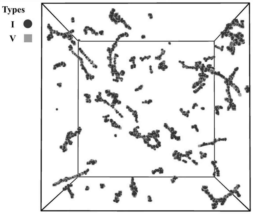
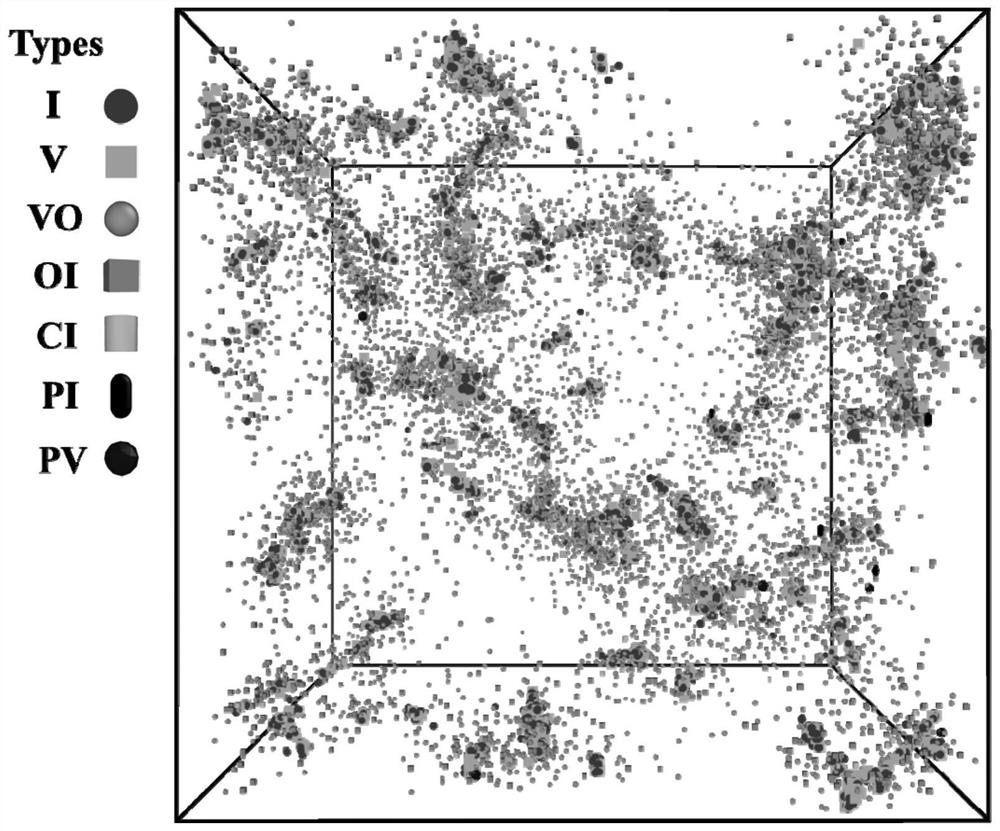
[0066] S20, calculating the spatial distribution of cas...


PUM


Abstract

The invention discloses a dynamic simulation method and device for carrier capture in an irradiated semiconductor. The method comprises the following steps: acquiring a defect reaction event and a parameter list in the semiconductor required by annealing; based on the defect reflection event and the parameter list, performing calculation to obtain cascaded defect space distribution after annealing; based on the annealed cascade defect space distribution, the radius of an effective cascade where the defect to be simulated is located and the average concentration of defects in the cascade are obtained; the radius and the average concentration of the defect to be simulated and the parameter list serve as input, the improved rate equation based on the SRH theory is solved, and the dynamic behavior of defect capture carriers is obtained. According to the method, the influence of the spatial heterogeneity of cascade defects and the complex cascade local potential on carrier capture is considered, more real defect distribution is adopted, the cascade local potential is strictly solved, and the dynamic behavior of capturing electrons / holes by deep-energy-level defects is accurately simulated without dependence or with little dependence on adjustable parameters as far as possible.

Description

technical field [0001] The invention relates to the technical field of semiconductors, in particular to a method and device for simulating the dynamics of carrier capture in an irradiated semiconductor. Background technique [0002] Semiconductor devices serving in space or nuclear energy environments are often exposed to high-energy neutron irradiation, resulting in the dislocation of lattice atoms of semiconductor materials, resulting in a series of irregular collision cascades of different sizes, and dislocation defects within the cascade. (Especially deep level defects) trap electrons / holes (carriers) and enhance the recombination of electrons and holes, resulting in reduced performance or even permanent failure of semiconductor devices. In addition, when the defects in the cascade trap carriers, they will form a local potential energy barrier near the cascade, thereby preventing the further trapping of carriers by the defects, which will further change the electrical pr...

Claims


Application Information

Patent Timeline
Patent Type & Authority Applications(China)
IPC IPC(8): G06F30/20G06F119/14G06F111/10
CPCG06F30/20G06F2119/14G06F2111/10
Inventor 曾雉刘俊
Owner HEFEI INSTITUTES OF PHYSICAL SCIENCE - CHINESE ACAD OF SCI
Features
  • R&D
  • Intellectual Property
  • Life Sciences
  • Materials
  • Tech Scout
  • Unparalleled Data Quality
  • Higher Quality Content
  • 60% Fewer Hallucinations
Learn More