Supercharge Your Innovation With Domain-Expert AI Agents!

Preparation device and preparation method of pixel definition layer

A technique for defining a pixel definition layer and preparing a device, which is applied in the display field, can solve problems such as reducing production efficiency and increasing manufacturing costs, and achieve the effects of improving production efficiency and saving equipment and material costs

Pending Publication Date: 2022-07-01
GUANGZHOU CHINA STAR OPTOELECTRONICS SEMICON DISPLAY TECH CO LTD
View PDF0 Cites 0 Cited by
  • Summary
  • Abstract
  • Description
  • Claims
  • Application Information

AI Technical Summary

Problems solved by technology

[0003] At present, the manufacturing process of the pixel definition layer is to first coat the material of the pixel definition layer, then expose and develop it through a mask plate, and finally perform etching to obtain the required pixel definition layer structure. This manufacturing process requires sophisticated exposure equipment and sophisticated Mask plate production increases manufacturing costs, and requires multiple manufacturing processes of coating, curing, exposure, development, and etching, reducing production efficiency

Method used


Image

  • Preparation device and preparation method of pixel definition layer
  • Preparation device and preparation method of pixel definition layer
  • Preparation device and preparation method of pixel definition layer

Examples


Embodiment Construction

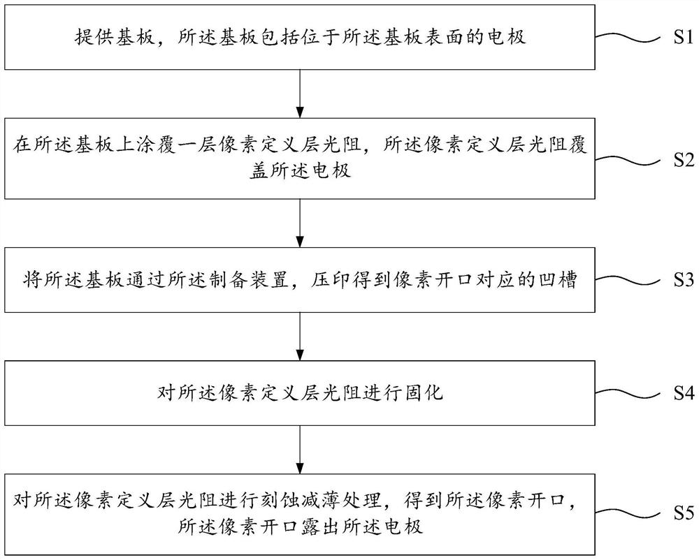
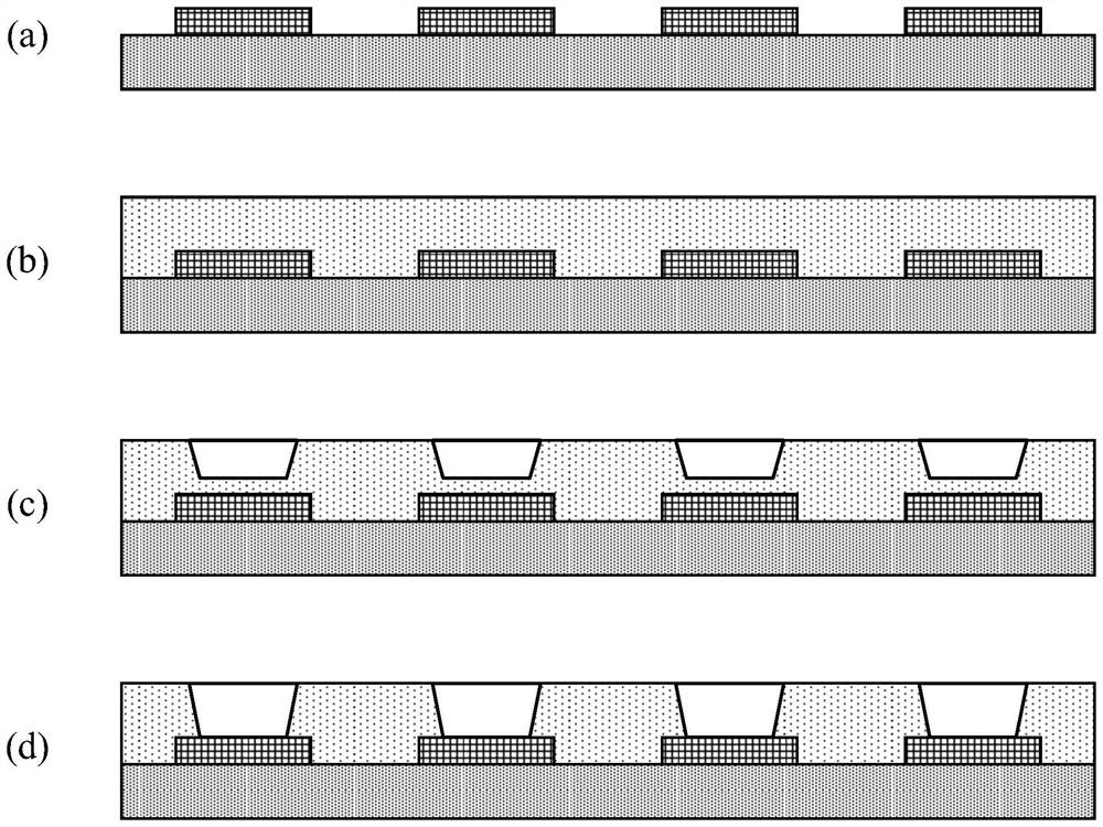
[0028] The following will clearly and completely describe the technical solutions in the embodiments and / or examples of the present invention in conjunction with the specific embodiments of the present invention. Obviously, the embodiments and / or examples described below are only part of the implementation of the present invention. Protocols and / or Examples, but not all embodiments and / or Examples. Based on the embodiments and / or examples in the present invention, all other embodiments and / or examples obtained by persons of ordinary skill in the art without creative efforts shall fall within the protection scope of the present invention.

[0029] The directional terms mentioned in the present invention, such as [up], [down], [left], [right], [front], [rear], [inner], [outer], [side], etc., are only for reference Additional schema orientation. Therefore, the directional terms used are for describing and understanding the present invention, not for limiting the present inventio...


PUM

PropertyMeasurementUnit
heightaaaaaaaaaa
thicknessaaaaaaaaaa

Abstract

The invention provides a preparation device and method of a pixel definition layer, and the device comprises a conveying unit which is used for conveying a substrate, and the substrate comprises a pixel definition layer light resistor which is located at one side, away from the conveying unit, of the substrate; and the imprint mold is arranged on one side, deviating from the conveying unit, of the substrate, and is used for imprint of the pixel definition layer photoresist to obtain a groove corresponding to a pixel opening. By adopting the preparation device provided by the embodiment of the invention and implementing the preparation method provided by the embodiment of the invention, the required pixel definition layer can be prepared on the substrate only through four technological processes of coating, imprinting, curing and etching; compared with the prior art in which a plurality of manufacturing technological processes of coating, curing, exposure, developing and etching are needed, and precise exposure equipment and a precise mask plate are needed, the manufacturing method has the advantages that the equipment and material cost in the preparation process of the pixel definition layer is saved, and the production efficiency of the pixel definition layer is improved.

Description

technical field [0001] The present application relates to the field of display, and in particular, to a preparation device and preparation method of a pixel definition layer. Background technique [0002] Organic Electroluminescence Display (OLED) and Quantum Dot Light Emitting Diodes (QLED) displays are fabricated by solution printing technology, which have the advantages of low cost, high productivity, and easy realization of large size, which is the future development of display technology. important direction. In the printing process, the pixel-defining layer is very important for the printing yield of the display material and the uniformity of the later film formation. [0003] At present, the manufacturing process of the pixel definition layer is to first coat the pixel definition layer material, then expose and develop through a mask, and finally etch to obtain the required pixel definition layer structure. This manufacturing process requires sophisticated exposure e...

Claims


Application Information

Patent Timeline
Patent Type & Authority Applications(China)
IPC IPC(8): H01L51/56H01L27/32G03F7/00
CPCG03F7/0002H10K59/122H10K71/00
Inventor 李楚曾宪甫刘礼瑜
Owner GUANGZHOU CHINA STAR OPTOELECTRONICS SEMICON DISPLAY TECH CO LTD
Features
  • R&D
  • Intellectual Property
  • Life Sciences
  • Materials
  • Tech Scout
  • Unparalleled Data Quality
  • Higher Quality Content
  • 60% Fewer Hallucinations
Learn More