Buffer welding pad, manufacturing method of buffer welding pad, chip and manufacturing method of chip

A manufacturing method and technology of bonding pads, which are applied in semiconductor/solid-state device manufacturing, semiconductor/solid-state device components, semiconductor devices, etc., can solve the problems of chip cracking, bonding pad cracking, weak bonding between metal wires and bonding pads, etc. , to reduce the risk of failure and improve reliability

Active Publication Date: 2022-07-22
BEIJING SMARTCHIP MICROELECTRONICS TECH COMPANY +1
View PDF8 Cites 0 Cited by
  • Summary
  • Abstract
  • Description
  • Claims
  • Application Information

AI Technical Summary

Problems solved by technology

[0002] In related technologies, after the wafer is cut into chips, a bonding process is usually used to connect the pads of the chip with external electronic components through metal wires. However, during the bonding process, if the bonding pressure is too small If the bonding pressure between the metal wire and the pad is too high, it will cause cracks in the pad and even crack the chip, which will also affect the reliability of the chip application. reliability

Method used


Image

  • Buffer welding pad, manufacturing method of buffer welding pad, chip and manufacturing method of chip
  • Buffer welding pad, manufacturing method of buffer welding pad, chip and manufacturing method of chip
  • Buffer welding pad, manufacturing method of buffer welding pad, chip and manufacturing method of chip

Examples


Embodiment Construction

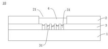
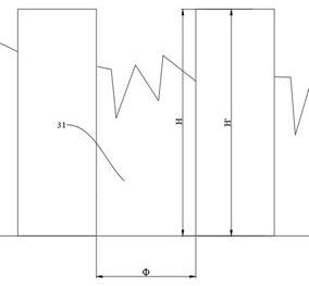
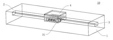
[0035] The following describes in detail the embodiments of the present invention, examples of which are illustrated in the accompanying drawings, wherein the same or similar reference numerals refer to the same or similar elements or elements having the same or similar functions throughout. The embodiments described below with reference to the accompanying drawings are exemplary, and are intended to explain the present invention and should not be construed as limiting the present invention.

[0036] In the description of the present invention, it should be understood that the orientation or positional relationship indicated by the terms "thickness", "upper", "lower", "inner", "outer", etc. are based on the orientation or positional relationship shown in the accompanying drawings , is only for the convenience of describing the present invention and simplifying the description, rather than indicating or implying that the indicated device or element must have a specific orientati...


PUM

PropertyMeasurementUnit
thicknessaaaaaaaaaa

Abstract

The invention discloses a buffer welding pad, a manufacturing method of the buffer welding pad, a chip and a manufacturing method of the chip. The buffer welding pad is used for a chip and comprises a first insulating layer, a second insulating layer, a first conductive layer and a second conductive layer, the second insulating layer is arranged above the first insulating layer, the second insulating layer is provided with a welding pad opening penetrating in the thickness direction, the first conductive layer is arranged between the first insulating layer and the second insulating layer, and the second conductive layer is arranged between the first insulating layer and the second insulating layer. The first conductive layer is provided with at least one buffer hole right below the welding pad hole, the second conductive layer is at least partially arranged in the welding pad hole, and the second conductive layer is conducted with the first conductive layer. According to the buffer welding pad provided by the embodiment of the invention, the first conductive layer is provided with at least one buffer hole right below the welding pad opening, so that when the buffer welding pad is connected with the metal wire in a binding manner, the pressure generated during binding is buffered, the risk of failure of the buffer welding pad is reduced, and the reliability of the buffer welding pad is improved.

Description

technical field [0001] The present invention relates to the technical field of chips, and in particular, to a buffer pad and a manufacturing method thereof, and a chip and a manufacturing method thereof. Background technique [0002] In the related art, after the wafer is cut into chips, the bonding process is usually used to connect the pads of the chip with external electronic components through metal wires. However, during the bonding process, if the bonding pressure is too small , the metal wire and the pad will not be bound firmly, which will affect the reliability of the chip application. If the bonding pressure between the metal wire and the pad is too large, the pad will crack, and even the chip will crack, which will also affect the reliability of the chip application. reliability. SUMMARY OF THE INVENTION [0003] The present invention aims to solve one of the above-mentioned technical problems in the prior art at least to a certain extent. Therefore, the first...

Claims


Application Information

Patent Timeline
Patent Type & Authority Applications(China)
IPC IPC(8): H01L23/488H01L23/485H01L21/60
CPCH01L23/485H01L24/11H01L24/13H01L2224/116H01L2224/11622
Inventor 张贺丰林杰杜君王文赫
Owner BEIJING SMARTCHIP MICROELECTRONICS TECH COMPANY
Why Eureka
Try Eureka