Flexible circuit board, manufacturing method thereof and display device

A technology for flexible circuit boards and display devices, which is used in printed circuit manufacturing, printed circuits, static indicators, etc. The effect of reliability

Pending Publication Date: 2022-07-26
BEIJING BOE OPTOELECTRONCIS TECH CO LTD +1
View PDF0 Cites 0 Cited by
  • Summary
  • Abstract
  • Description
  • Claims
  • Application Information

AI Technical Summary

Problems solved by technology

[0004] The present invention provides a flexible circuit board, a manufacturing method thereof, and a display device to solve the existing problem that only signal traces are formed on a flexible substrate, and when the display device is hit, the flexible circuit board is easily torn.

Method used


Image

  • Flexible circuit board, manufacturing method thereof and display device
  • Flexible circuit board, manufacturing method thereof and display device
  • Flexible circuit board, manufacturing method thereof and display device

Examples


Embodiment 1

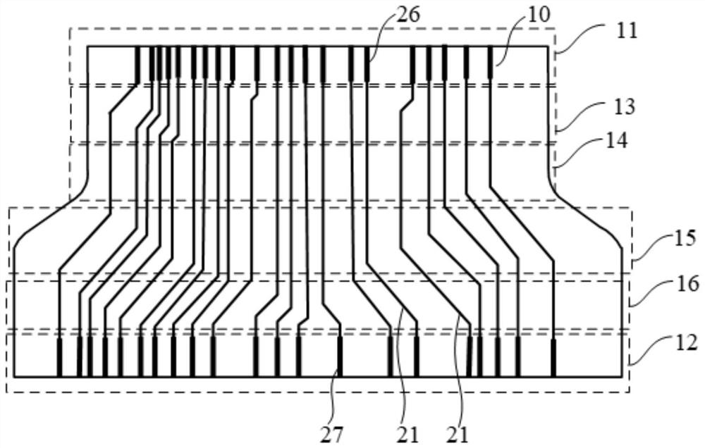
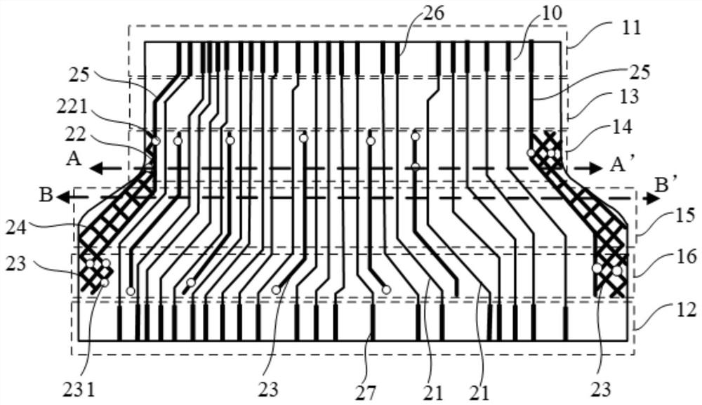
[0039] refer to figure 1 , showing a schematic structural diagram of the first surface of a flexible circuit board according to an embodiment of the present invention, figure 2 A schematic structural diagram of the second surface of the flexible circuit board according to the embodiment of the present invention is shown.

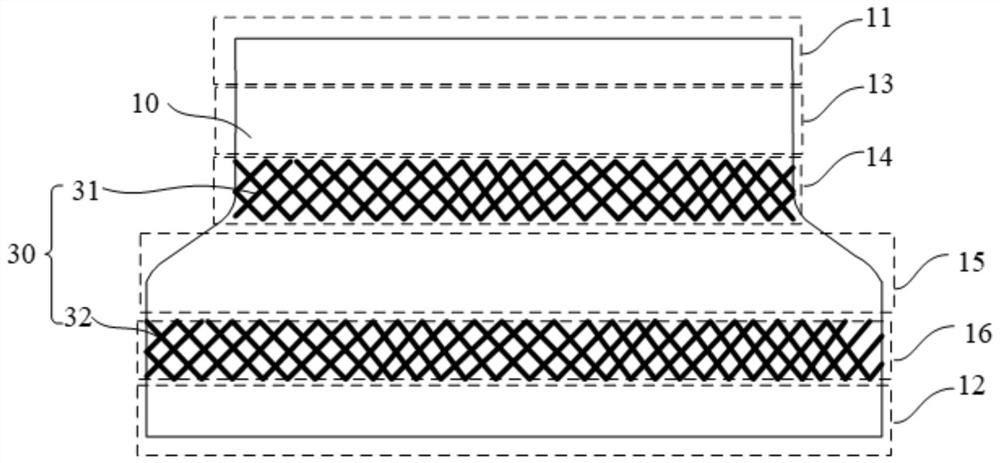
[0040] An embodiment of the present invention provides a flexible circuit board, the flexible circuit board includes a flexible substrate 10, and the flexible substrate 10 is divided into a wiring area and a first binding area 11 and a second binding area on both sides of the wiring area 12. The routing area includes a first routing area 13, a second routing area 14, a third routing area 15 and a fourth routing area 16 that are in turn away from the first binding area 11; the flexible circuit board also includes a The wiring layer on the flexible substrate 10 and the reinforcing layer 30 arranged on the side of the flexible substrate 10 away from the wirin...

Embodiment 2

[0074] refer to Image 6 , showing a flow chart of a method for manufacturing a flexible circuit board according to an embodiment of the present invention, which may specifically include the following steps:

[0075] Step 601, providing a flexible substrate; the flexible substrate is divided into a routing area and a first binding area and a second binding area on both sides of the routing area, the routing area includes The first routing area, the second routing area, the third routing area and the fourth routing area of ​​the first binding area.

[0076] In the embodiment of the present invention, first, a flexible substrate 10 is provided, and according to the fixing method and fixing position of the flexible circuit board in the display device, the flexible circuit board is divided into a wiring area and a first binding area on both sides of the wiring area. A fixed area 11 and a second binding area 12 , and the routing area includes a first routing area 13 , a second rou...

Embodiment 3

[0087] Embodiments of the present invention provide a display device, such as Figure 7 As shown, it includes a display panel 71 , a printed circuit board 72 and the above-mentioned flexible circuit board 73 , and the flexible circuit board 73 is bound to the display panel 71 and the printed circuit board 72 respectively.

[0088] The display panel 71 is bound to the first gold finger 26 in the first binding area 11 of the flexible circuit board 73 , and the printed circuit board 72 is bound to the first gold finger 26 in the second binding area 12 of the flexible circuit board 73 . Two golden fingers are bound to 27.

[0089] For the specific description of the flexible circuit board 73, reference may be made to the descriptions of the first and second embodiments above, and details are not repeated here.

[0090] In addition, the display device further includes a cover plate and a backlight module, the cover plate covers the light-emitting surface of the display panel 71, a...


PUM


Abstract

The invention provides a flexible circuit board, a manufacturing method thereof and a display device, and relates to the technical field of display. A wiring layer is arranged on a flexible substrate, a reinforcing layer is further arranged on the side, away from the wiring layer, of the flexible substrate, and the wiring layer comprises a plurality of signal wires distributed along a first wiring area, a second wiring area, a third wiring area and a fourth wiring area; the reinforcing layer comprises a first reinforcing structure located in the second wiring area and a second reinforcing structure located in the fourth wiring area. The first reinforcing structure is arranged in the second wiring area of the flexible substrate, and the second reinforcing structure is arranged in the fourth wiring area of the flexible substrate, so that the anti-impact strength of the flexible circuit board is enhanced, and therefore, when the display device is impacted, the flexible circuit board is not easy to tear, normal use of the display device is ensured, and the service life of the display device is prolonged. And the yield and the reliability of the display device are improved.

Description

technical field [0001] The present invention relates to the field of display technology, in particular to a flexible circuit board, a manufacturing method thereof, and a display device. Background technique [0002] In a display device, it is usually necessary to use an FPC (Flexible Printed Circuit, flexible circuit board) to realize the circuit connection between the display panel and a PCB (Printed Circuit Board, printed circuit board). [0003] At present, the flexible circuit board forms signal traces on the surface of one side of the flexible substrate. When the display device is impacted, the flexible circuit board is easily torn, so that the display device cannot be used normally. SUMMARY OF THE INVENTION [0004] The present invention provides a flexible circuit board, a manufacturing method thereof, and a display device, so as to solve the problem that the existing signal wiring is only formed on a flexible substrate, and the flexible circuit board is easily torn...

Claims


Application Information

Patent Timeline
Patent Type & Authority Applications(China)
IPC IPC(8): H05K1/02H05K3/40G09G3/20
CPCH05K1/028H05K1/0281H05K3/40G09G3/20G02F1/13452H05K1/0219H05K1/189H05K2201/10128H05K1/0393H05K3/24G02F1/133608G02F1/133308H05K3/4652
Inventor 王晓霞冷寿阳马青韩锐于洁崔栋李鹏涛赵铁磊王春华董小乔王遥遥于静
Owner BEIJING BOE OPTOELECTRONCIS TECH CO LTD
Why Eureka
Try Eureka