Organic compound, light-emitting device, light-emitting device, electronic device, and lighting device
A technology of organic compounds and formulas, applied in the field of organic compounds, to achieve the effect of low power consumption and high reliability
- Summary
- Abstract
- Description
- Claims
- Application Information
AI Technical Summary
Problems solved by technology
Method used
Image
Examples
Embodiment approach 1
[0114] 1,1-bis[4-[N,N-bis(p-tolyl)amino] is known as one of materials having a low refractive index among organic compounds having carrier transport properties that can be used in organic EL devices Phenyl]cyclohexane (abbreviation: TAPC). When a material with a low refractive index is used for the EL layer, the external quantum efficiency of the light-emitting device can be improved, so it is expected that a light-emitting device having a good external quantum efficiency can be obtained by using TAPC. However, since TAPC has a low glass transition point, it has a problem with heat resistance. In addition, TAPC can flow holes, but substantially cannot flow electrons.
[0115] Note that, in order to obtain a material with a low refractive index, it is preferable to introduce an atom having a small atomic refraction or a substituent having a low molecular refraction into the molecule. A saturated hydrocarbon group, a cyclic saturated hydrocarbon group, etc. are mentioned as a ...
Embodiment approach 2
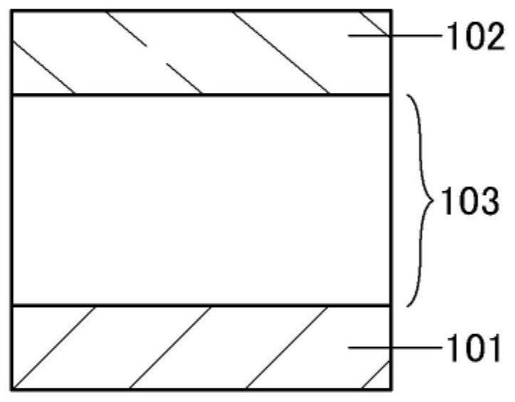
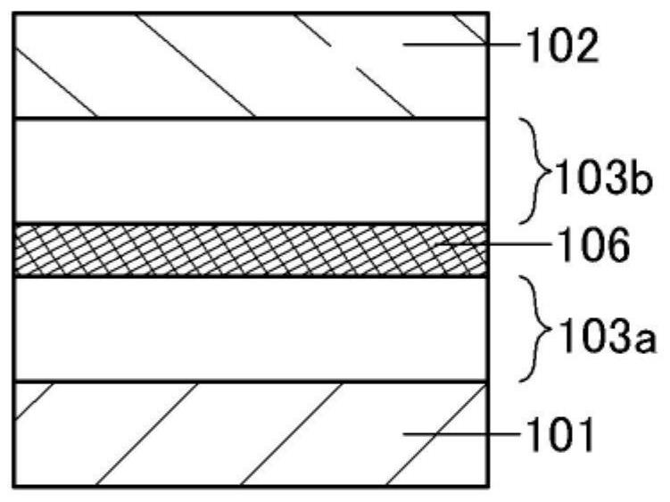
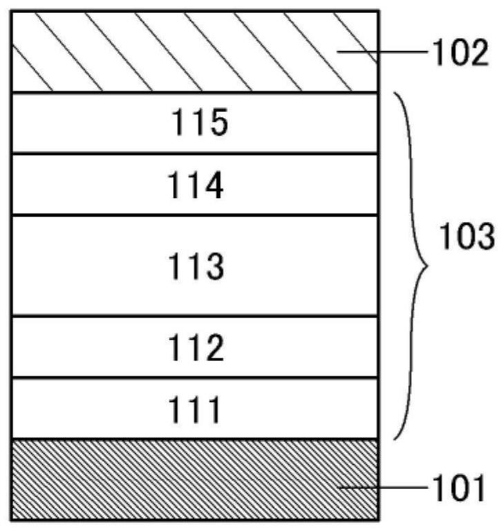
[0251] In this embodiment, refer to 1A to 1E A light-emitting device using the organic compound shown in Embodiment 1 will be described.
[0252] >
[0253] exist 1A to 1E In the light-emitting device shown, Figure 1A and Figure 1C The light-emitting device shown has a structure (single structure) in which an EL layer is sandwiched between a pair of electrodes, whereas, Figure 1B , Figure 1D and Figure 1E It is a structure (tandem structure) in which a charge generating layer is sandwiched between an EL layer sandwiched between a pair of electrodes, and two or more layers are stacked. Note that the structure of the EL layer is the same in both structures. Furthermore, in Figure 1D In the case where the illustrated light-emitting device has a microcavity structure, a reflective electrode is formed as the first electrode 101 , and a semi-transmissive / semi-reflective electrode is formed as the second electrode 102 . Thus, the above-mentioned electrodes can be forme...
Embodiment approach 3
[0361] In this embodiment mode, a specific configuration example and a manufacturing method of a light-emitting device (also referred to as a display panel) according to one embodiment of the present invention will be described.
[0362]
[0363] Figure 2A The illustrated light emitting device 700 includes a light emitting device 550B, a light emitting device 550G, a light emitting device 550R, and a partition wall 528 . In addition, the light emitting device 550B, the light emitting device 550G, the light emitting device 550R, and the partition wall 528 are formed on the functional layer 520 provided on the first substrate 510 . The functional layer 520 includes, in addition to the driver circuit GD, the driver circuit SD, the pixel circuit, and the like, which are constituted by a plurality of transistors, wiring and the like for electrically connecting them. Note that, as an example, these driving circuits are electrically connected to the light emitting device 550B, th...
PUM
| Property | Measurement | Unit |
|---|---|---|
| glass transition temperature | aaaaa | aaaaa |
| glass transition temperature | aaaaa | aaaaa |
| length | aaaaa | aaaaa |
Abstract
Description
Claims
Application Information


