

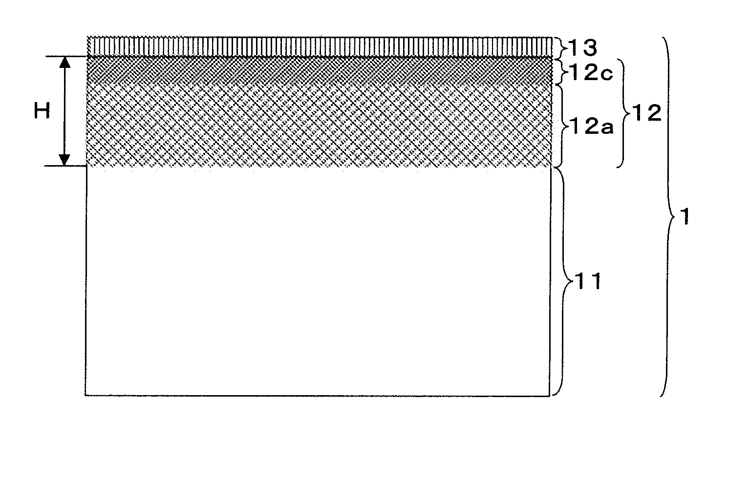
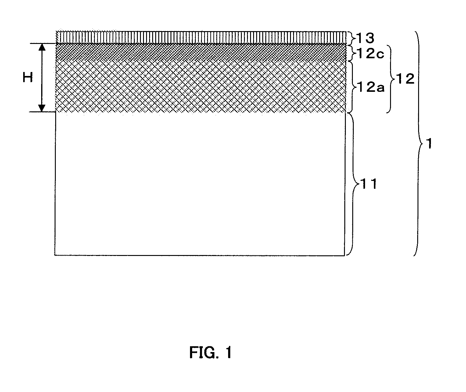
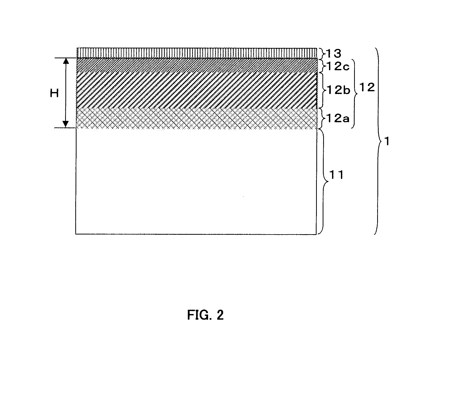
Anti-Reflection Film And Manufacturing Method Thereof
a technology of anti-reflection film and manufacturing method, which is applied in the direction of polarising elements, instruments, transportation and packaging, etc., can solve the problems of low productivity, reduced display quality, and hard coat layer made by curing acrylic materials, so as to reduce material costs, reduce total usage of conductive particles, and achieve sufficient anti-static
- Summary
- Abstract
- Description
- Claims
- Application Information
AI Technical Summary
Benefits of technology
Problems solved by technology
Method used
Image

Examples
example 1
Transparent Substrate
[0187]An 80 μm thick triacetyl cellulose film was prepared as the transparent substrate.
[0188]4.0 parts by weight of a dispersion liquid of antimony-doped tin oxide particles (ATO, average particle diameter: 8 nm, solid content ratio: 30 wt %, dispersion solvent: isopropyl alcohol) as the conductive particles, 7.8 parts by weight of dipentaerythritol hexaacrylate (DPHA), 7.8 parts by weight of pentaerythritol tetraacrylate (PETA) and 23.3 parts by weight of urethane acrylate UA-306T (made by Kyoeisha chemical Co., Ltd.) as the ionizing radiation curable material, 2.0 parts by weight of Irgacure 184 (by Ciba Japan) as the photopolymerization initiator, and 57.2 parts by weight of a solvent mixture of methyl ethyl ketone, dimethyl carbonate and diacetone alcohol having a blend ratio of 4:4:2 as the solvent were blended together to prepare a coating liquid for forming an antistatic hard coat layer with a solid content ratio of 40 wt % by weight.
[0189]The resultant ...
example 2
Transparent Substrate
[0192]An 80 μm thick triacetyl cellulose film was prepared as the transparent substrates.
[0193]1.7 parts by weight of a dispersion liquid of antimony-doped tin oxide particles (ATO, average particle diameter: 8 nm, solid content ratio: 30 wt %, dispersion solvent: isopropyl alcohol) as the conductive particles, 4.9 parts by weight of dipentaerythritol hexaacrylate (DPHA), 4.9 parts by weight of pentaerythritol tetraacrylate (PETA) and 14.7 parts by weight of urethane acrylate UA-306T (made by Kyoeisha chemical Co., Ltd.) as the ionizing radiation curable material, 1.5 parts by weight of Irgacure 184 (by Ciba Japan) as the photopolymerization initiator, and 73.8 parts by weight of a solvent mixture of methyl ethyl ketone, dimethyl carbonate and diacetone alcohol having a blend ratio of 4:4:2 as the solvent were blended together to prepare a coating liquid for forming an antistatic hard coat layer with a solid content ratio of 25 wt % by weight.
[0194]The resultant...
example 3
Transparent Substrate
[0197]An 80 μm thick triacetyl cellulose film was prepared as the transparent substrate.
[0198]4.0 parts by weight of a dispersion liquid of antimony-doped tin oxide particles (ATO, average particle diameter: 20 nm, solid content ratio: 30 wt %, dispersion solvent: isopropyl alcohol) as the conductive particles, 7.8 parts by weight of dipentaerythritol hexaacrylate (DPHA), 7.8 parts by weight of pentaerythritol tetraacrylate (PETA) and 23.3 parts by weight of urethane acrylate UA-306T (made by Kyoeisha chemical Co., Ltd.) as the ionizing radiation curable material, 2.0 parts by weight of Irgacure 184 (by Ciba Japan) as the photopolymerization initiator, and 57.2 parts by weight of a solvent mixture of methyl ethyl ketone, dimethyl carbonate and diacetone alcohol having a blend ratio of 4:4:2 as the solvent were blended together to prepare a coating liquid for forming an antistatic hard coat layer with a solid content ratio of 40 wt % by weight.
[0199]The resultant...
PUM
| Property | Measurement | Unit |
|---|---|---|
| optical thickness | aaaaa | aaaaa |
| optical thickness | aaaaa | aaaaa |
| thickness | aaaaa | aaaaa |
Abstract
Description
Claims
Application Information