

Display device
A display device and electrode technology, which is applied to semiconductor devices, electrical components, circuits, etc., can solve the problems of performance deterioration of display components, uneven ends of functional layers, etc.
- Summary
- Abstract
- Description
- Claims
- Application Information
AI Technical Summary
Problems solved by technology
Method used
Image

Examples
no. 1 approach
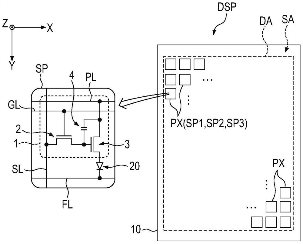
[0044] figure 1 It is a figure which shows an example of a structure of the display apparatus DSP concerning 1st Embodiment. The display device DSP has a display area DA on which an image is displayed, and a peripheral area SA outside the display area DA on the insulating base material 10 . The substrate 10 may be glass or a flexible resin film.
[0045] The display area DA includes a plurality of pixels PX arranged in a matrix along the first direction X and the second direction Y. The pixel PX includes a plurality of sub-pixels SP. In one example, the pixel PX includes a red sub-pixel SP1, a green sub-pixel SP2, and a blue sub-pixel SP3. In addition, the pixel PX may include four or more sub-pixels to which sub-pixels of other colors such as white are added, in addition to the sub-pixels of the above three colors.
[0046] The sub-pixel SP includes a pixel circuit 1 and a display element 20 driven by the pixel circuit 1 . The pixel circuit 1 includes a pixel switch 2 , ...
no. 2 approach
[0097] Figure 15 It is a schematic plan view of the organic layer OR of the second embodiment. Figure 16 is along the Figure 15 A schematic cross-sectional view of the display device DSP along the line XVI-XVI. exist Figure 15 in, with Figure 5 Similarly, in the first direction X of the sub-pixel SP (display element 20 ), the shape of the organic layer in plan view OR is shown in the region on the left side of the center line CL, and the region on the right side of the center line CL shows the shape of the organic layer. Outlines of the layers 51 to 57 of the layer OR and the opening OP.
[0098] Figure 15 The organic layers shown are OR with Figure 5 The organic layer OR shown is different in that the area of the second carrier blocking layer 55 is larger than that of the first carrier blocking layer 53 . When viewed from above, the ends S1 and S2 are located between the ends S3 and S4, the end S3 is located between the ends S1, S2 and the end S5, and the end ...
no. 3 approach
[0102] Figure 17 It is a schematic cross-sectional view of the display device DSP according to the third embodiment. exist Figure 17 In the example, the first carrier transport layer 52 covers the end S1 of the first carrier injection layer 51, the first carrier blocking layer 53 covers the end S2 of the first carrier transport layer 52, the light emitting layer 54 covers the end S3 of the first carrier blocking layer 53 , the second carrier blocking layer 55 covers the end S4 of the light emitting layer 54 , and the second carrier transport layer 56 covers the end S4 of the second carrier blocking layer 55 . At the end S5 , the second carrier injection layer 57 covers the end S6 of the second carrier transport layer 56 . In each of the layers 51 to 57 , the portions near the end portions S1 to S7 are in contact with the rib portion 14 . The second carrier injection layer 57 is in contact with the second electrode E2 as a whole, but the other layers 51 to 56 are not in co...
PUM
 Abstract
Description
Claims
Application Information