Supercharge Your Innovation With Domain-Expert AI Agents!

Composite circuit board and manufacturing method thereof

A manufacturing method and circuit board technology, which are applied in the directions of printed circuit components, secondary processing of printed circuits, reinforcement of conductive patterns, etc., can solve problems such as sacrificial circuit layout

Pending Publication Date: 2022-07-29
TRIPOD WUXI ELECTRONICS
View PDF5 Cites 0 Cited by
  • Summary
  • Abstract
  • Description
  • Claims
  • Application Information

AI Technical Summary

Problems solved by technology

However, the heat dissipation structure used by existing circuit boards to achieve high heat dissipation requirements often needs to sacrifice the circuit layout (for example: the circuit layout needs to bypass the above heat dissipation structure)

Method used


Image

  • Composite circuit board and manufacturing method thereof
  • Composite circuit board and manufacturing method thereof
  • Composite circuit board and manufacturing method thereof

Examples


Embodiment 1

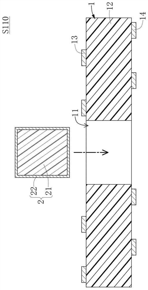
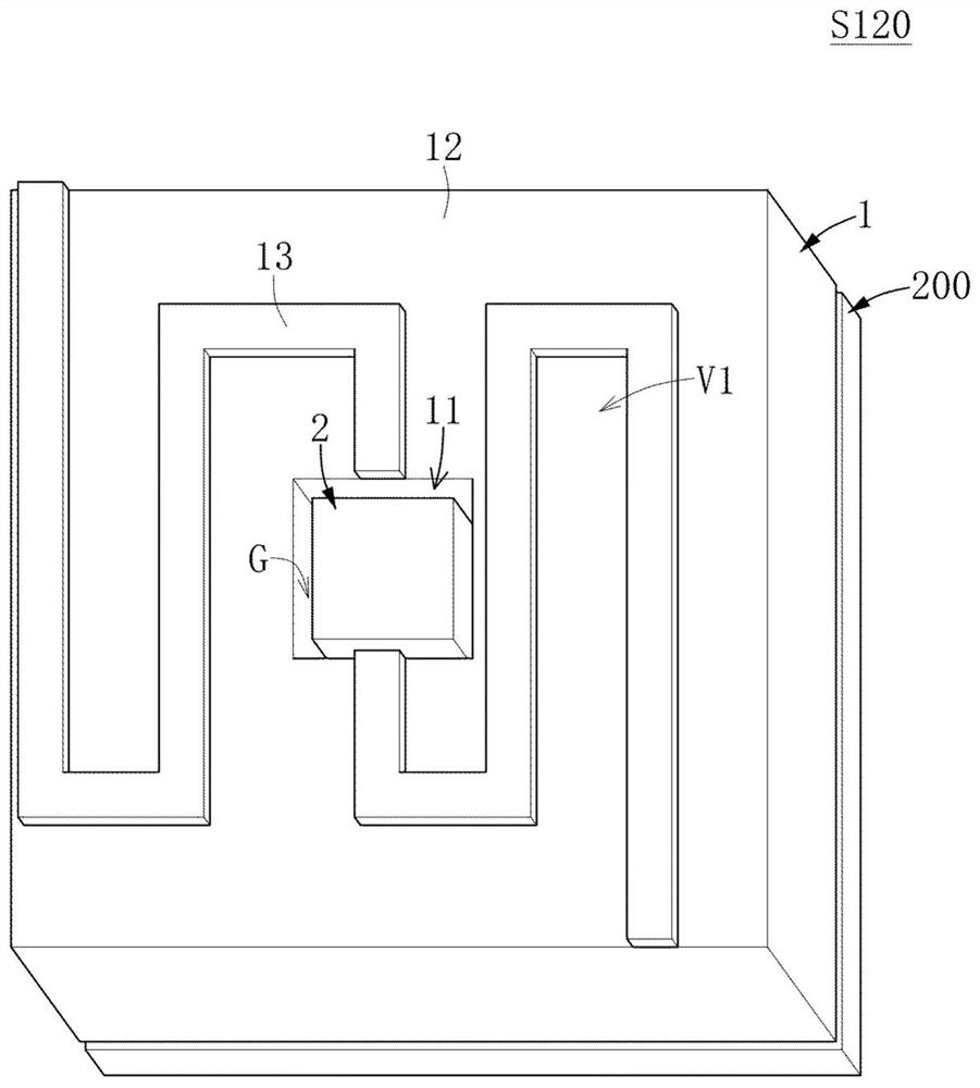
[0051] see Figure 1 to Figure 9 As shown, it is the first embodiment of the present invention. This embodiment discloses a composite circuit board 100 and a method for manufacturing the same. To facilitate the description of this embodiment, the following first describes the method for manufacturing the composite circuit board, and then describes the composite circuit board 100 . Wherein, the composite circuit board 100 is manufactured by implementing the manufacturing method of the composite circuit board in this embodiment, but the present invention is not limited thereto.

[0052] see Figure 1 to Figure 9 As shown, it is a schematic flowchart of the manufacturing method of the composite circuit board. Wherein, the manufacturing method of the composite circuit board in this embodiment sequentially includes a preparation step S110, an insertion step S120, a printing step S130, a thickening step S140, a planarization step S150, and an electroplating step. S160, and a patt...

Embodiment 2

[0076] see Figure 10 and Figure 11 As shown, it is the second embodiment of the present invention. Since this embodiment is similar to the above-mentioned first embodiment, the similarities between the two embodiments will not be repeated, and the differences between this embodiment and the first embodiment are roughly described as follows:

[0077] In this embodiment, the ceramic block 2 does not include the conductive layer 22 in the first embodiment; that is, the ceramic block 2 in this embodiment is equivalent to the ceramic body 21 in the first embodiment. Accordingly, the first circuit extension area 221 is defined on the surface of the ceramic block 2 adjacent to the first circuit layer 13 and exposed outside the insulating ink 3 (eg: Figure 11 The top surface of the ceramic block 2 in the middle), and the second circuit addition area 222 is defined on the surface of the ceramic block 2 adjacent to the second circuit layer 14 and exposed outside the insulating ink ...


PUM


Abstract

The invention discloses a composite circuit board and a manufacturing method thereof. The composite circuit board comprises a substrate, a ceramic block, insulating ink and a first additional circuit. The substrate is provided with a board body, a first circuit layer formed on one side of the board body, and a second circuit layer formed on the other side of the board body. A through containing hole is formed in the substrate, and the ceramic block is located in the containing hole and fixed to the hole wall of the containing hole through the insulating ink. The first additional circuit is connected with and coplanar with the first circuit layer, and the first additional circuit is formed on the ceramic block.

Description

technical field [0001] The invention relates to a circuit board, in particular to a composite circuit board and a manufacturing method thereof. Background technique [0002] As the application of high calorific value products is becoming more and more popular, the requirements for the heat dissipation efficiency and heat resistance of circuit boards are also getting higher and higher. Therefore, in recent years, thermally conductive circuit boards have been gradually applied to high calorific value products to meet the heat dissipation efficiency and heat resistance requirements of high calorific value products. However, the heat dissipation structure adopted by the existing circuit boards to achieve high heat dissipation requirements often requires sacrificing the circuit layout (for example, the circuit layout needs to bypass the above heat dissipation structure). [0003] Therefore, the inventors of the present invention believe that the above-mentioned defects can be im...

Claims


Application Information

Patent Timeline
IPC IPC(8): H05K3/24H05K1/09
CPCH05K3/247H05K1/09H05K2201/0364H05K2203/04
Inventor 吕政明石汉青范字远陈文哲胡魏雄
Owner TRIPOD WUXI ELECTRONICS
Features
  • R&D
  • Intellectual Property
  • Life Sciences
  • Materials
  • Tech Scout
  • Unparalleled Data Quality
  • Higher Quality Content
  • 60% Fewer Hallucinations
Learn More