Packaging structure and display device

A packaging structure and package technology, applied in semiconductor devices, electrical components, photovoltaic power generation, etc., can solve problems such as driver chip signal interference, achieve the effect of improving signal shielding ability, reducing signal interference, and improving performance

Pending Publication Date: 2022-08-05
BRIGHTEK OPTOELECTRONICS CO LTD (JIANGSU)
View PDF0 Cites 0 Cited by
  • Summary
  • Abstract
  • Description
  • Claims
  • Application Information

AI Technical Summary

Problems solved by technology

[0005] The purpose of this application is to provide a packaging structure and a display device, which can solve the technical problem of signal interference of the drive chip in the prior art

Method used


Image

  • Packaging structure and display device
  • Packaging structure and display device
  • Packaging structure and display device

Examples


Embodiment 1

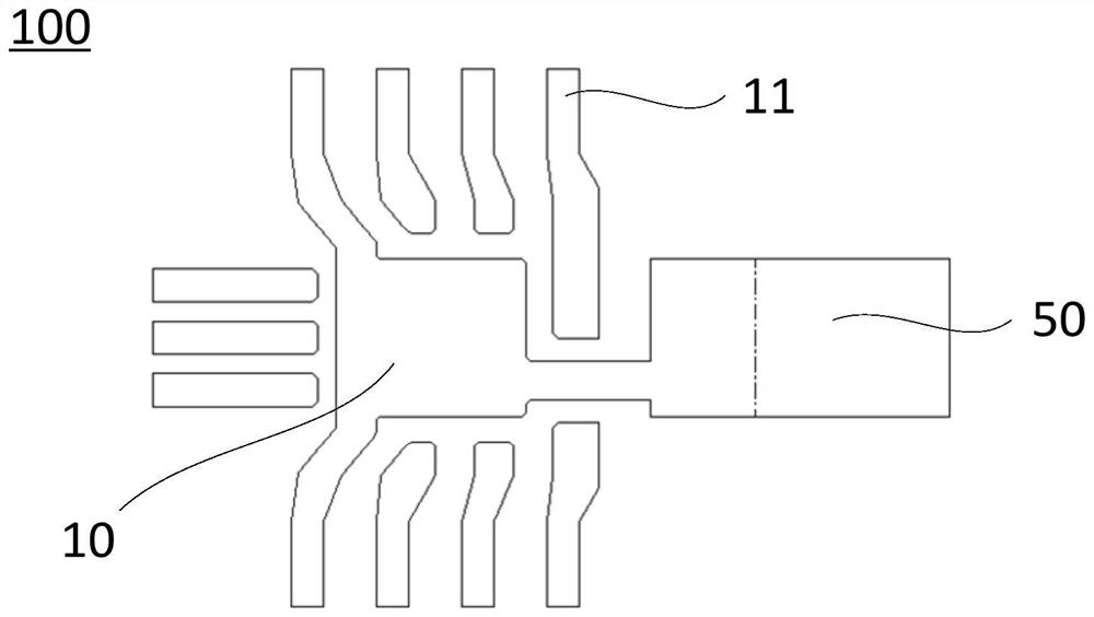
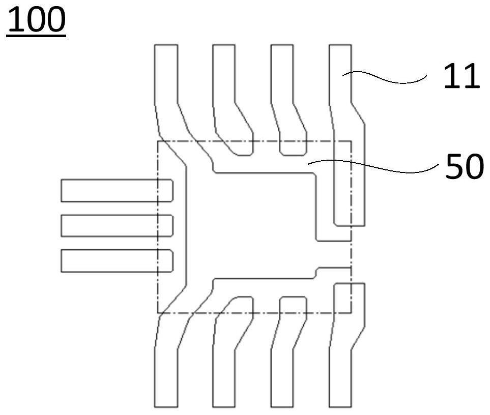
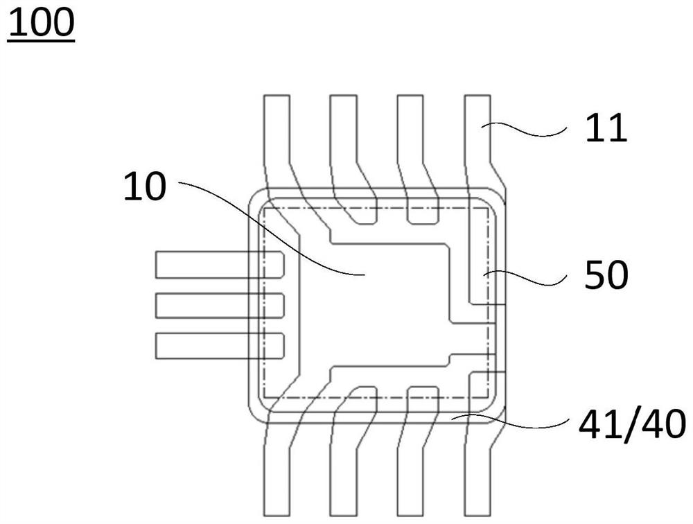
[0039] like Figure 1-Figure 8 As shown, the embodiment of the present application provides a package structure 100 , which includes a metal bracket 10 , a driving chip 20 , a light-emitting component 30 , a package 40 and a metal cover plate 50 .

[0040] like figure 1 , Figure 5 and Figure 7 As shown, the metal bracket 10 includes several pins 11 and oppositely disposed first surfaces (eg, Figure 5 The side shown in A) and the second side (for example Figure 5 side shown in B).

[0041] like Figure 5 and Figure 7 As shown, the driving chip 20 is disposed on the first surface of the metal bracket 10 , and the driving chip 20 is used to control the light-emitting state of the light-emitting element 30 . Specifically, the driving chip 20 is configured to receive an external electrical signal, and send the control information carried by the electrical signal to the light-emitting component 30 .

[0042] like Figure 5 , Image 6 and Figure 7As shown, the light-...

Embodiment 2

[0063] like Figure 9-Figure 13 As shown, the embodiment of the present application provides a package structure 100 , which includes a metal bracket 10 , a driving chip 20 , a light-emitting component 30 , a package 40 and a metal cover plate 50 .

[0064] In the examples provided in this application, such as Figure 9 , Figure 10 and Figure 13 As shown, the metal bracket 10 includes several pins 11 and oppositely disposed first surfaces (eg, Figure 9 side shown) and the second side (e.g. Figure 13 The side shown), wherein the driving chip 20 is arranged on the first side, the light-emitting element 30 is arranged on the second side, and the light-emitting element 30 is electrically connected to the driving chip 20 through the metal bracket 10, and the driving chip 20 is used to control the light emission Lighted state of assembly 30. The package 40 is disposed on the metal bracket 10 , fixes the metal bracket 10 and covers the driving chip 20 and the light-emitting ...

Embodiment 3

[0075] The present application provides a display device including a circuit board and a plurality of packaging structures 100 . The plurality of packaging structures 100 are disposed on the circuit board and are arranged in a matrix.

[0076] The display device provided by the present application can improve the performance of the display device and reduce the occupation area of ​​the packaging structure 100 in the display device by improving the packaging structure 100 . Specifically, in the package structure 100 provided by the present application, by improving the structure of the metal bracket 10 and arranging the metal cover plate 50 on the side of the driver chip 20 away from the light-emitting component 30 , the driver chip 20 is located in the metal bracket 10 and several pins 11 In the space formed by the metal cover plate 50 and the package structure 100 , the signal shielding capability of the package structure 100 can be improved, thereby improving the use stabilit...


PUM


Abstract

The invention relates to the technical field of semiconductors, and discloses a packaging structure and a display device. The packaging structure comprises a metal support, a driving chip, a light-emitting assembly, a packaging piece and a metal cover plate. Wherein the metal support comprises a plurality of pins, a first face and a second face, the first face and the second face are oppositely arranged, the driving chip is arranged on the first face of the metal support and used for controlling the light-emitting state of the light-emitting assembly, and the light-emitting assembly is arranged on the second face of the metal support and electrically connected with the driving chip through the metal support. The packaging piece is arranged on the metal support, the packaging piece fixes the metal support and wraps the driving chip and the light-emitting assembly, the pins surround the driving chip and are partially exposed out of the packaging piece, and the metal cover plate is arranged on the side, away from the light-emitting assembly, of the driving chip and covers the whole driving chip. According to the packaging structure and the display device provided by the invention, the signal interference problem of the driving chip in the prior art can be solved, so that the use performance of a product is greatly improved.

Description

technical field [0001] The present application relates to the field of semiconductor technology, and in particular, to a packaging structure and a display device. Background technique [0002] Light-emitting diode (LED) is a solid-state semiconductor device that can convert electrical energy into visible light. It uses a solid semiconductor chip as a light-emitting material, and releases energy through the recombination of carriers, causing photon emission and directly converting electrical energy. for light energy. [0003] LED light sources are widely used in the field of display technology due to their advantages of high brightness, small size, low energy consumption and high stability. Among them, the key to improving the resolution of the LED display is to reduce the size of the LED packaging unit. [0004] In the related art, in order to reduce the size of the LED packaging unit, a vertical packaging structure is designed, that is, the LED chip and the driving chip a...

Claims


Application Information

Patent Timeline
Patent Type & Authority Applications(China)
IPC IPC(8): H01L25/16H01L33/54H01L33/62
CPCH01L25/167H01L33/54H01L33/62Y02E10/50H01L33/486H01L25/0753
Inventor 吴锋曾智宏黄建中
Owner BRIGHTEK OPTOELECTRONICS CO LTD (JIANGSU)
Why Eureka
Try Eureka