

Electron-emitting device, electron source and image-forming apparatus as well as method of manufacturing the same
A technology for electron emission and emission devices, which is applied in the fields of electrical components, cold cathode manufacturing, electrode system manufacturing, etc., and can solve the problems of low efficiency and complex process.
Inactive Publication Date: 2004-09-08
CANON KK
View PDF2 Cites 0 Cited by
- Summary
- Abstract
- Description
- Claims
- Application Information
AI Technical Summary
Problems solved by technology
The disadvantage is that the process is c
Method used
View moreImage
Smart ImageViewing Examples

Examples
 PUM
| Property | Measurement | Unit |
|---|---|---|
| Thickness | aaaaa | aaaaa |
| Thickness | aaaaa | aaaaa |
| Resistance | aaaaa | aaaaa |
Abstract
The invention provides a method for making electron-emitting device which includes a pair of electrodes and an electroconductive film arranged between the electrodes and including an electron-emitting region, and which is characterized by including a step for applying voltage on the electroconductive film having gap in a gas environment which contains no less than one kind of organic compounds and a component which can be represented by general formula XY (wherein X and Y respectively represent hydrogen atom and halogen atom).
Description
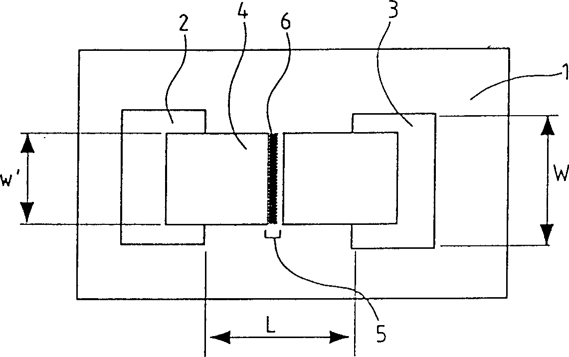
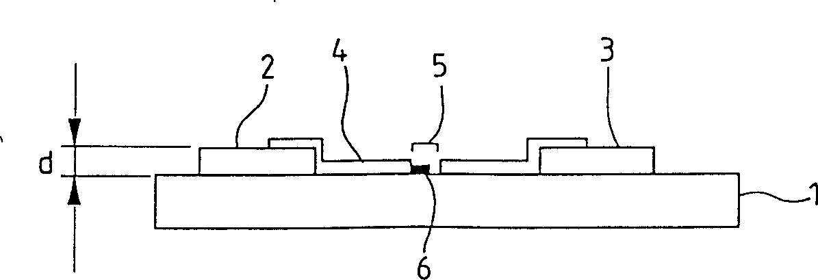
[0001] This application is a divisional application filed on August 29, 1995, with application number 95116828.2, and the title of the invention is "Electron Emitting Device, Electron Source, Image Forming Device and Manufacturing Method". technical field [0002] The present invention relates to a method of manufacturing an electron-emitting device and a method of manufacturing an electron source and an image forming apparatus such as a display apparatus or an exposure apparatus including the electron-emitting device. Background technique [0003] Known electron-emitting devices are of two types: hot cathode type and cold cathode type. Among them, cold cathode emission types include field emission type (hereinafter referred to as FE type) devices, metal / insulator / metal type (hereinafter referred to as MIM type) electron emission devices, and surface conduction electron emission devices. Examples of FE-type devices include those proposed by W.P. Dyke & W.W. Dolan, see "Field...
Claims
Login to View More Application Information
Patent Timeline
 IPC IPC(8): H01J1/316H01J9/02
CPCH01J9/027H01J31/127H01J2329/0489H01J2201/3165H01J2329/00H01J29/481H01J1/316
Inventor 岸文夫山野边正人冢本健夫大西敏一山本敬介池田外充浜元康弘宫崎和也
Owner CANON KK