Constructed integrated circuit with balance structure

A technology of integrated circuits and balanced structures, applied in circuits, electrical components, electrical solid-state devices, etc., can solve the problems of thermal stress concentration, uneven stress distribution, warpage of assembled integrated circuits, etc., to reduce the volume and avoid thermal stress. The effect of concentration, improving stability and yield

Inactive Publication Date: 2005-04-27
VIA TECH INC
View PDF0 Cites 0 Cited by
  • Summary
  • Abstract
  • Description
  • Claims
  • Application Information

AI Technical Summary

Problems solved by technology

Since multiple chips with different volumes and weights are implanted on the substrate, in the process of circuit design, the stress distribution on the substrate and the thermal stress effect are often not taken into consideration in order to improve the performance of the integrated circuit.
When the chips on the substrate go through a assembling process to form a structured integrated circuit, during the operation of the structured integrated circuit, due to heat generation and partial concentration, warpage will easily occur due to uneven stress distribution on the substrate. curved defect
This warping defect will not only affect the operation performance of the assembled integrated circuit, but also ca

Method used


Image

  • Constructed integrated circuit with balance structure
  • Constructed integrated circuit with balance structure
  • Constructed integrated circuit with balance structure

Examples


Example Embodiment

The specific implementation of the present invention will be described in detail below in conjunction with the drawings and embodiments.

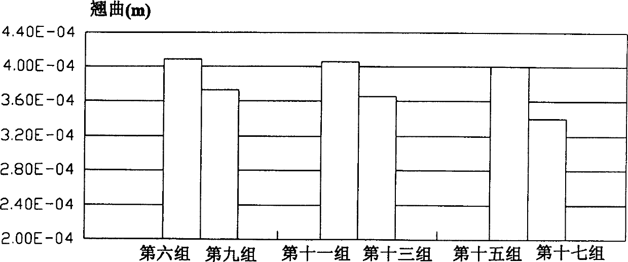
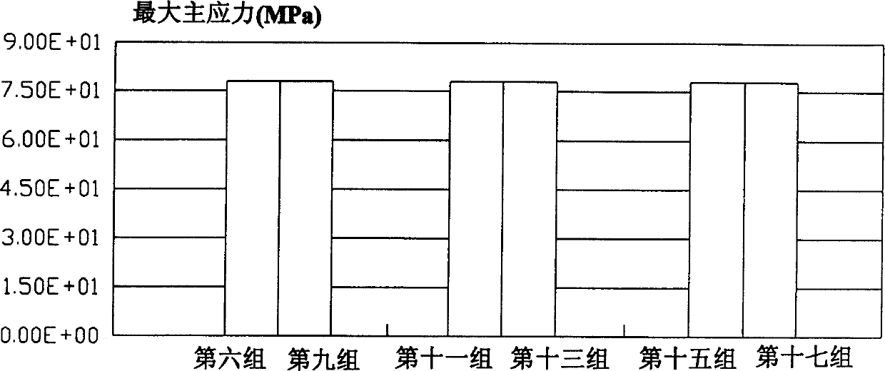
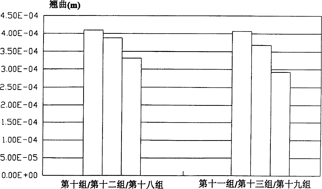
The present invention provides a balanced structure installed in a packaged integrated circuit, which utilizes balanced modules arranged on a substrate to reduce the degree of warpage of the packaged integrated circuit. Referring to Figure 1 and Figure 2, this is a schematic diagram of the integrated circuit before the process of assembling the potting mold mixture. The chips 100 and 102 can be connected to the substrate by a plurality of solder bumps 110 (refer to FIG. 1). The chips 100 and 102 can also be bonded to the substrate 120 by the bonding layers 150 and 152, and then go through a wire bonding process to connect the chips 100 and 102 to the substrate 120 by a plurality of metal wires 154 (refer to FIG. 2 ). Referring to Figures 3 and 4, this is a schematic diagram of an integrated circuit that connects a plurality of balance modules on ...


PUM


Abstract

This invention relates to an IC with balance structure. It is first to see the thermal stress distribution situation resulted by quantity, position and weight of chips connected to the baseboard to decide to mount how many balance modules to balance the stress distribution situation on IC constitutive before adhering radiating plates or constitutive glued module mixers to reduce thermal stress effect i the IC structure to avoid the shortcoming of warping.

Description

technical field The present invention relates to a packaged integrated circuit, in particular to a packaged integrated circuit with a balanced structure. Background technique Integrated circuits generally need to be built in packaging materials, such as the traditional Quad Flat Package (QFP). The flat package structure includes a lead frame on which there are a number of leads that make contact with the integrated circuit chip. The chip is housed in a strong plastic that is mechanically supported and insulated from the circuit, while the leads are primarily soldered to the printed circuit board. In the past, integrated circuit manufacturers have developed integrated circuit packaging technologies to meet the miniaturization requirements. The improvement method for miniaturized integrated circuits is to enable it to combine millions of transistor circuit components including circuits, chips, etc. on a silicon substrate. These improved methods have led to a greater empha...

Claims


Application Information

Patent Timeline
IPC IPC(8): H01L25/065H01L25/16H01L25/18
CPCH01L2224/73204H01L2224/16225
Inventor 何昆耀宫振越顾诗章廖学国
Owner VIA TECH INC
Why Eureka
Try Eureka