ITO sputtering target
A technology of sputtering target and sputtering surface, which is applied in the field of ITO sputtering target, and can solve problems such as inability to suppress arc
- Summary
- Abstract
- Description
- Claims
- Application Information
AI Technical Summary
Problems solved by technology
Method used
Image
Examples
Embodiment 1
[0039] Will In 2 o 3 Powder and SnO 2 powder with In 2 o 3 :SnO 2 = 90:10% by mass, mixed with an ITO sintered body by a common method, and used as a target. This target material is cut into the size of φ 4 inches, then grinds the surface (sputtering surface) that is used for sputtering and the surface (adhesive surface) that are used for bonding with the plane grinder disc these two sides, it is adjusted to 6 Micron thickness, followed by grinding the sputtered surface with a diamond grinder.
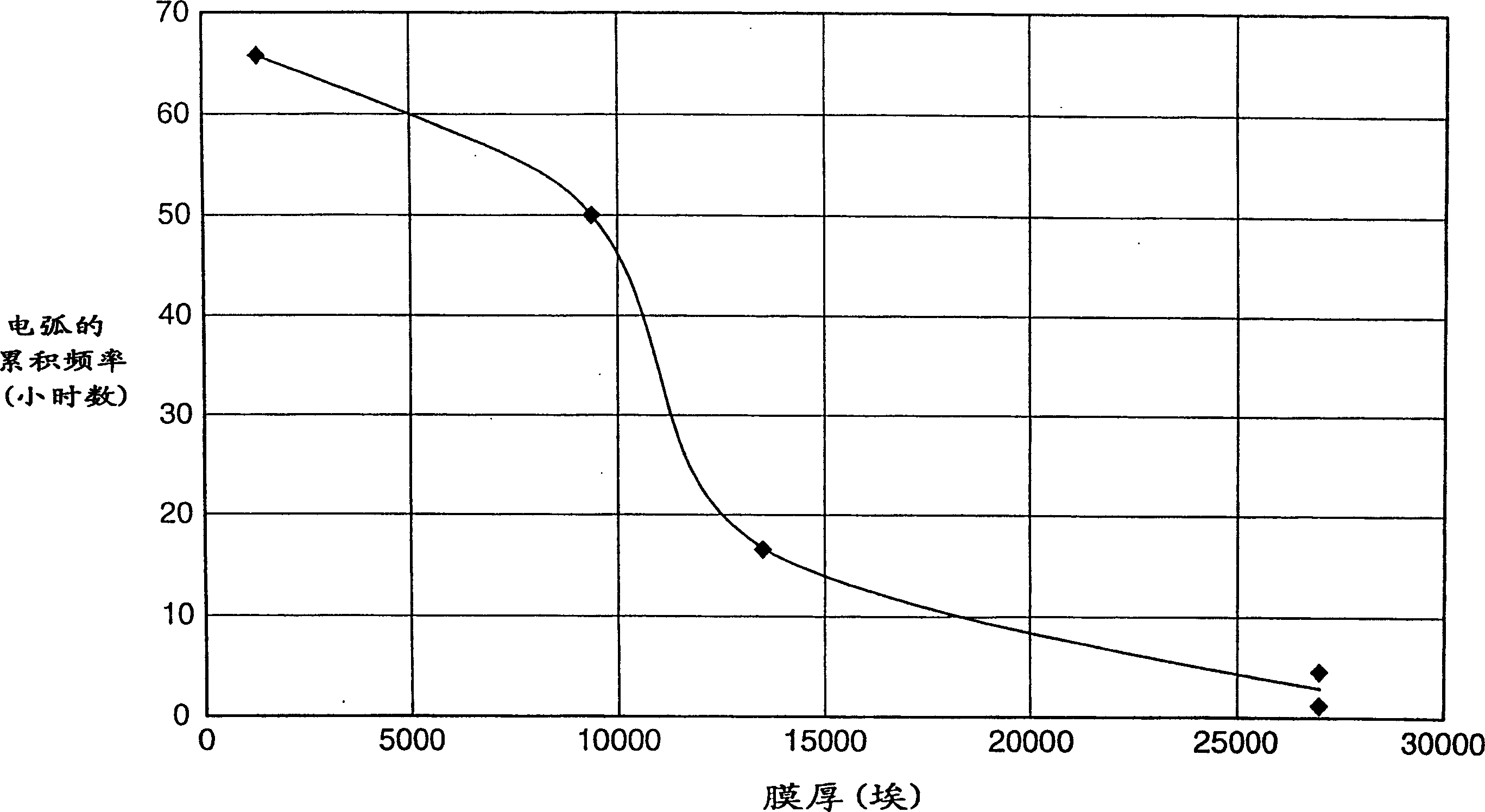
[0040] The target is set on the anode side of the sputtering device, another ITO target is set on the cathode side, and sputtering is carried out under the following conditions, and the sputtering surface of the target on the anode side is plated to form a film thickness of 135000 angstroms (1.35 microns ) of the ITO film.
[0041] The sputtering conditions and sputtering methods at this time are: DC magnetron sputtering machine, process gas: Ar, process pressure: 3 mTorr, oxyge...
Embodiment 2
[0044] Except making the film thickness of the ITO film that forms on the sputtering surface of target material be 27000 angstroms (2.7 micron, all the other make target according to the method identical with embodiment 1. Measure ITO film with the method identical with embodiment 1 Surface roughness before and after plating formation. The results are shown in Table 1.
Embodiment 3
[0046] In addition to roughly grinding the two sides of the sputtering surface and the bonding surface of the target with a flat grinding disc, after adjusting it to a thickness of 6 mm, sandblasting was performed with aluminum beads instead of grinding the sputtering surface with a diamond grinder, and The target was prepared in the same manner as in Example 1 except that the thickness of the ITO film formed by plating on the sputtering surface of the target was 27000 Angstroms (2.7 microns). The surface roughness before and after the ITO film plating formation was measured by the same method as in Example 1. The results are shown in Table 1.
PUM
| Property | Measurement | Unit |
|---|---|---|
| thickness | aaaaa | aaaaa |
| thickness | aaaaa | aaaaa |
| surface roughness | aaaaa | aaaaa |
Abstract
Description
Claims
Application Information
 - R&D Engineer
- R&D Manager
- IP Professional
- Industry Leading Data Capabilities
- Powerful AI technology
- Patent DNA Extraction
Browse by: Latest US Patents, China's latest patents, Technical Efficacy Thesaurus, Application Domain, Technology Topic, Popular Technical Reports.
© 2024 PatSnap. All rights reserved.Legal|Privacy policy|Modern Slavery Act Transparency Statement|Sitemap|About US| Contact US: help@patsnap.com


