
Manufacturing method of self-aligned metallic silicide with improved electric characteristics on contact surface

A technology of metal silicide and manufacturing method, applied in semiconductor/solid-state device manufacturing, circuits, electrical components, etc., can solve the problems of rising resistance value, easy agglomeration of cobalt silicide, and high reaction consumption ratio

Inactive Publication Date: 2005-09-14
GRACE SEMICON MFG CORP
View PDF0 Cites 0 Cited by
  • Summary
  • Abstract
  • Description
  • Claims
  • Application Information

AI Technical Summary

Problems solved by technology

But for cobalt metal silicide, there are two serious disadvantages. One is that when cobalt metal silicide is formed, it consumes more silicon than other metal silicides that get the same resistance value, that is, the reaction between silicon and cobalt The reaction consumption ratio of forming cobalt silicide is as high as 3.6, that is, one unit of cobalt must be reacted with 3.6 units of silicon to form cobalt silicide. is a serious shortcoming
Another disadvantage is that cobalt metal cannot eliminate oxides at the interface like titanium, which makes the surface of the substrate more important; and if there are oxidized impurities on the surface of polysilicon or the substrate, the silicide of cobalt and its silicon after the reaction Cobalt is easy to agglomerate, resulting in an accelerated rise in resistance

Method used


Image

  • Manufacturing method of self-aligned metallic silicide with improved electric characteristics on contact surface
  • Manufacturing method of self-aligned metallic silicide with improved electric characteristics on contact surface
  • Manufacturing method of self-aligned metallic silicide with improved electric characteristics on contact surface

Examples


Embodiment Construction

[0016] As far as the known technology is concerned, during the fabrication of cobalt metal silicide, it is easy to produce self-generated or residual oxide or any impurity on the surface of the source / drain region, thereby causing cluster shrinkage and shallow junction leakage. The present invention proposes a preferred process step to improve the electrical characteristics of the junction between the self-aligned metal silicide and the source / drain region.

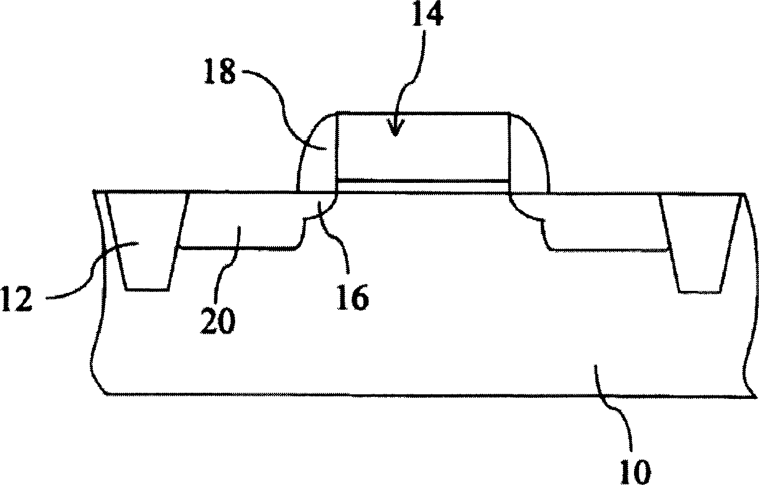
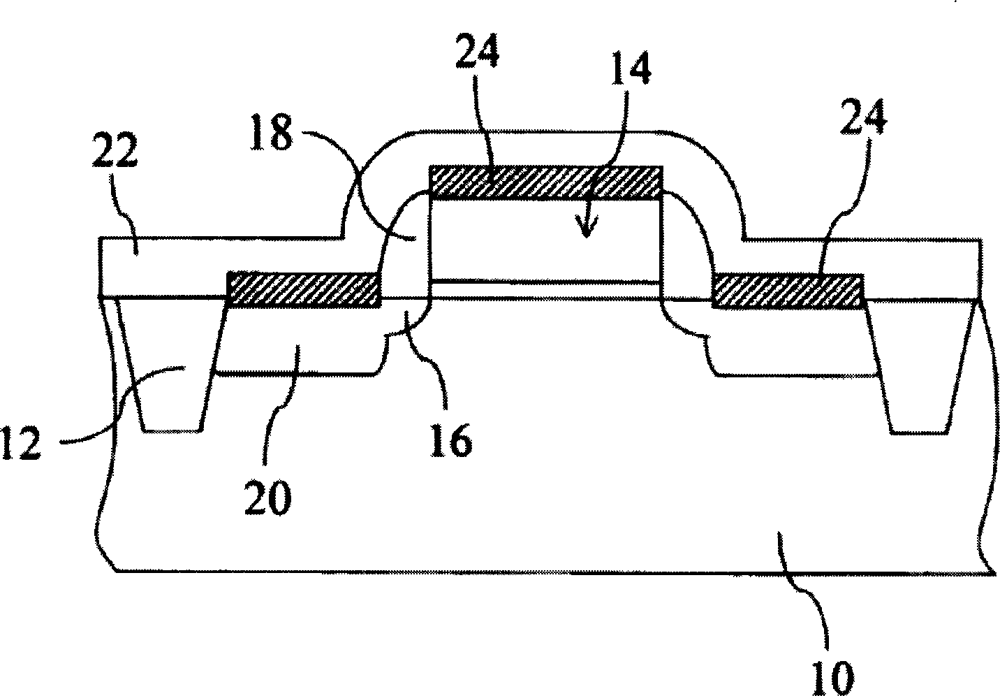
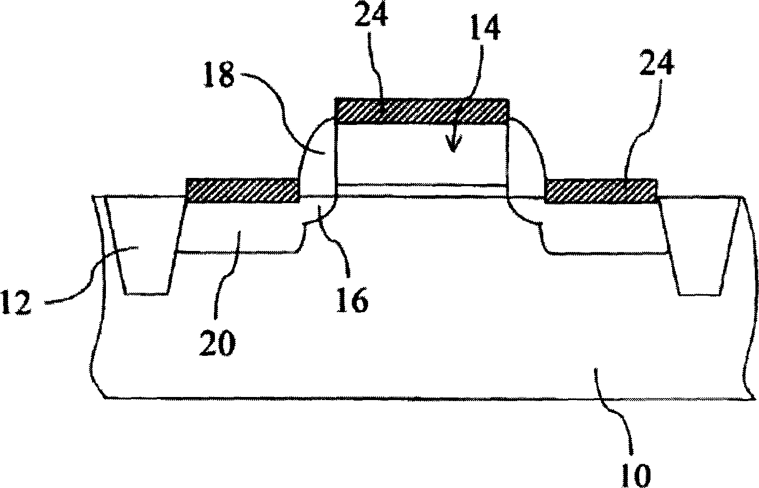
[0017] Figure 2(a) to Figure 2(d) It is a cross-sectional view of the structure of each step of making self-aligned metal silicide in the present invention. First, as shown in FIG. To isolate the active components and passive components in the semiconductor substrate 30; and then form a transistor gate structure 34 on the surface of the semiconductor substrate 30, which is composed of a gate oxide layer 342 on the surface of the semiconductor substrate and a polysilicon layer 344 above it; Then, using the gate structure...


PUM

PropertyMeasurementUnit
thicknessaaaaaaaaaa
thicknessaaaaaaaaaa
thicknessaaaaaaaaaa

Abstract

The present invention discloses a method for making a self-aligned metal silicate which can improve the electrical property of the contacting surface. The method comprises the processes of forming a metal layer on a semiconductor substrate after forming isolating area, gate structure, lightly doped source / drain areas and gate clearance barrier; carrying out a high dose ion implantation to form the heavily doped source / drain areas; and then making the self-aligned metal silicate. It can be used in semiconductor devices with the dimension smaller than sub-micron while improving effectively electrical properties of metal silicate and shallow contacting surface.

Description

technical field [0001] The present invention relates to a method for making self-aligned silicide (SALICIDE), in particular to a self-aligned method that can improve the electrical properties of metal silicide and source / drain junctions Method for producing metal silicides. Background technique [0002] When the size of semiconductor components shrinks to the deep sub-micron range, the areas of the gate and source / drain regions are also reduced, so that the conduction resistance on the gate and the contact resistance of the source / drain regions are greatly increased. At this time, it is necessary to use a A self-aligned metallization is formed to reduce the resistance. Generally, metals that can be used for self-aligned metal silicides include titanium, cobalt, nickel, palladium, and platinum. These metals can be self-aligned by a second annealing treatment and a selective solution etching treatment in between. The purpose of the metalloid silicide reaction. [0003] The ...

Claims


Application Information

Patent Timeline
Patent Type & Authority Patents(China)
IPC IPC(8): H01L21/28H01L21/3205H01L21/336
Inventor 高荣正
Owner GRACE SEMICON MFG CORP
Learn More