
Static discharge protection circuit and relative metal oxide semiconductor transistor structure

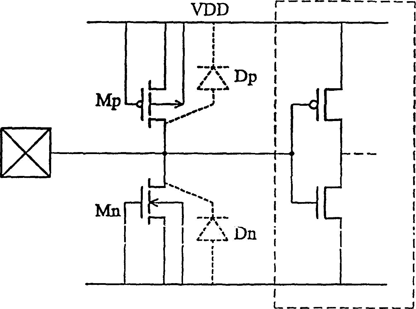
An electrostatic discharge protection, bipolar junction transistor technology, applied in semiconductor devices, semiconductor/solid-state device components, circuits, etc., can solve problems such as inability to increase, and achieve the best ESD protection effect.

Inactive Publication Date: 2006-02-08
TAIWAN SEMICON MFG CO LTD
View PDF0 Cites 0 Cited by
  • Summary
  • Abstract
  • Description
  • Claims
  • Application Information

AI Technical Summary

Problems solved by technology

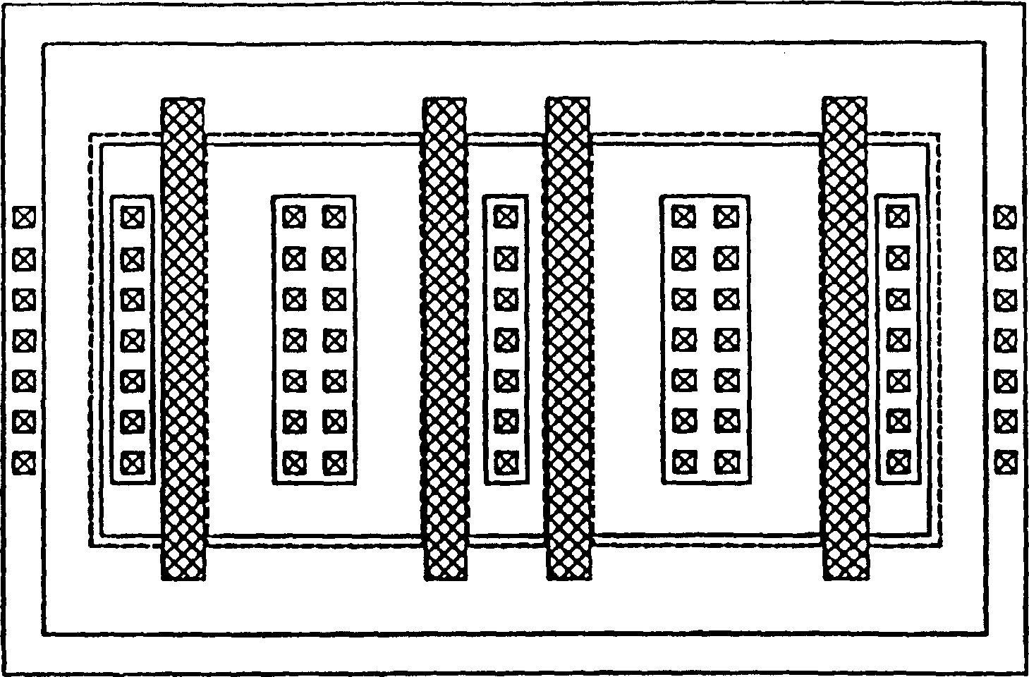
Moreover, often only some of the few finger gates are triggered
Therefore, the ESD resistance of multi-finger structure MOS often cannot increase with the increase of component size.

Method used


Image

  • Static discharge protection circuit and relative metal oxide semiconductor transistor structure
  • Static discharge protection circuit and relative metal oxide semiconductor transistor structure
  • Static discharge protection circuit and relative metal oxide semiconductor transistor structure

Examples


Embodiment Construction

[0030] Figure 5 It is the ESD protection circuit triggered by the substrate of the present invention, which is illustrated by the concept of NMOS implementation picture . The ESD protection circuit 30 of the present invention has a multi-finger NMOS (G1-Gn finger structure), multiple transient current detection elements 32 and multiple feedback circuits 34 . A finger drain of each finger structure is coupled to a bonding pad 36 . Each transient current detection element 32 is coupled between a finger source of a finger structure and a Vss power line. The finger drain, base and finger source under each finger structure respectively constitute a collector, base and emitter of a parasitic BJT (T1-Tn). Each feedback circuit (feedback circuits) 34 is connected between the emitter of one parasitic BJT and the base of another parasitic BJT, such as Figure 5 shown.

[0031] The main principle of the present invention is as follows. If the multi-finger NMOS is not evenly trigg...


PUM


Abstract

Protection circuit of electro-static discharge (ESD) includes a component possessing polydactyly structure, multiple components for measuring transient state current and multiple feedback line. The component of polydactyly structure possesses finger grids, finger source electrode and at least one drain electrode, which is coupled to a joint mat. A bipolarity junction transistor (BJT) is parasitized under each finger grid. Each finger source electrode is emitter of one of BJT. Each transient state current measuring component is coupled between relevant finger source electrode and a power source line in order to detect transient state current passing through relevant finger grid. Each feedback line is coupled between base electrode of first BJT and emitter of second BJT in order to trigger the first BJT to discharge ESD current, if ESD event occurs.

Description

technical field [0001] The invention relates to an electrostatic discharge (ESD) protection circuit and its related components, in particular to an ESD protection circuit with high matrix trigger efficiency. Background technique [0002] Basically, ESD is an instantaneous energy release process in which a large amount of external energy passes through an integrated circuit (integrated circuit), and the entire discharge process is about 100 nanoseconds. In such a short period of time, hundreds of volts, or even thousands of volts of ESD stress have to be released. If the release process is not appropriate, it will easily cause damage to the components in the IC, especially the gate of the transistor. As the thickness of the gate oxide layer shrinks, the gate is more fragile, and the IC needs to be specially designed to prevent possible damage caused by ESD. [0003] The release of a large amount of energy is bound to cause hyperthermia. Considering the effect of heat dissi...

Claims


Application Information

Patent Timeline
Patent Type & Authority Patents(China)
IPC IPC(8): H01L23/60H01L29/78
Inventor 柯明道徐国钧
Owner TAIWAN SEMICON MFG CO LTD
Learn More