
High frequency switch circuit

一种高频开关、高频的技术,应用在电路、电子开关、电气元件等方向,能够解决导通开关导通电阻增加等问题,达到增加处理功率、减少传输损耗的效果

Inactive Publication Date: 2006-07-05
NEC CORP
View PDF0 Cites 0 Cited by
  • Summary
  • Abstract
  • Description
  • Claims
  • Application Information

AI Technical Summary

Problems solved by technology

If the Vgs of the non-conducting switch increases negatively to increase the conducting power, the on-resistance of the conducting switch increases

Method used

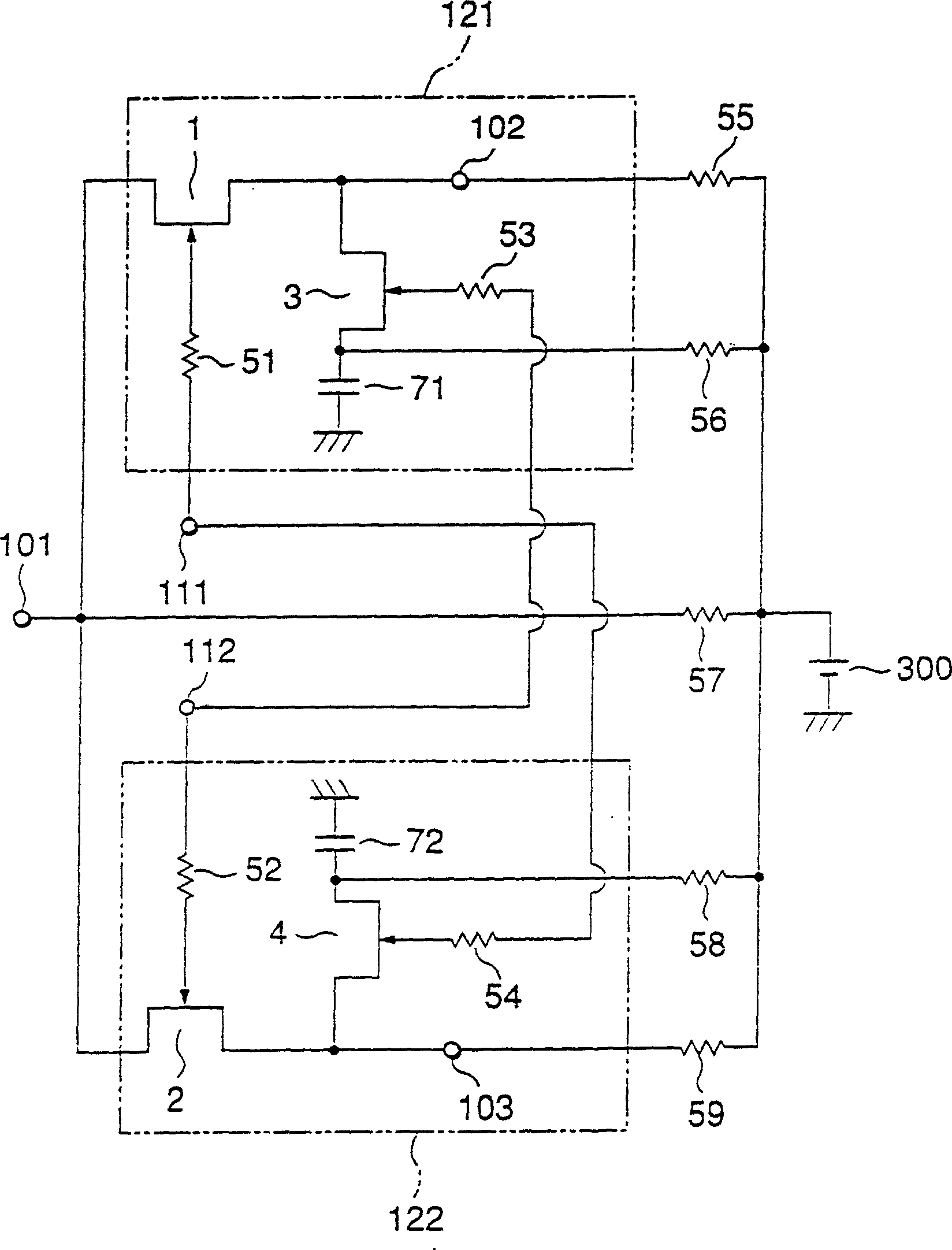

Image

  • High frequency switch circuit
  • High frequency switch circuit
  • High frequency switch circuit

Examples


Embodiment Construction

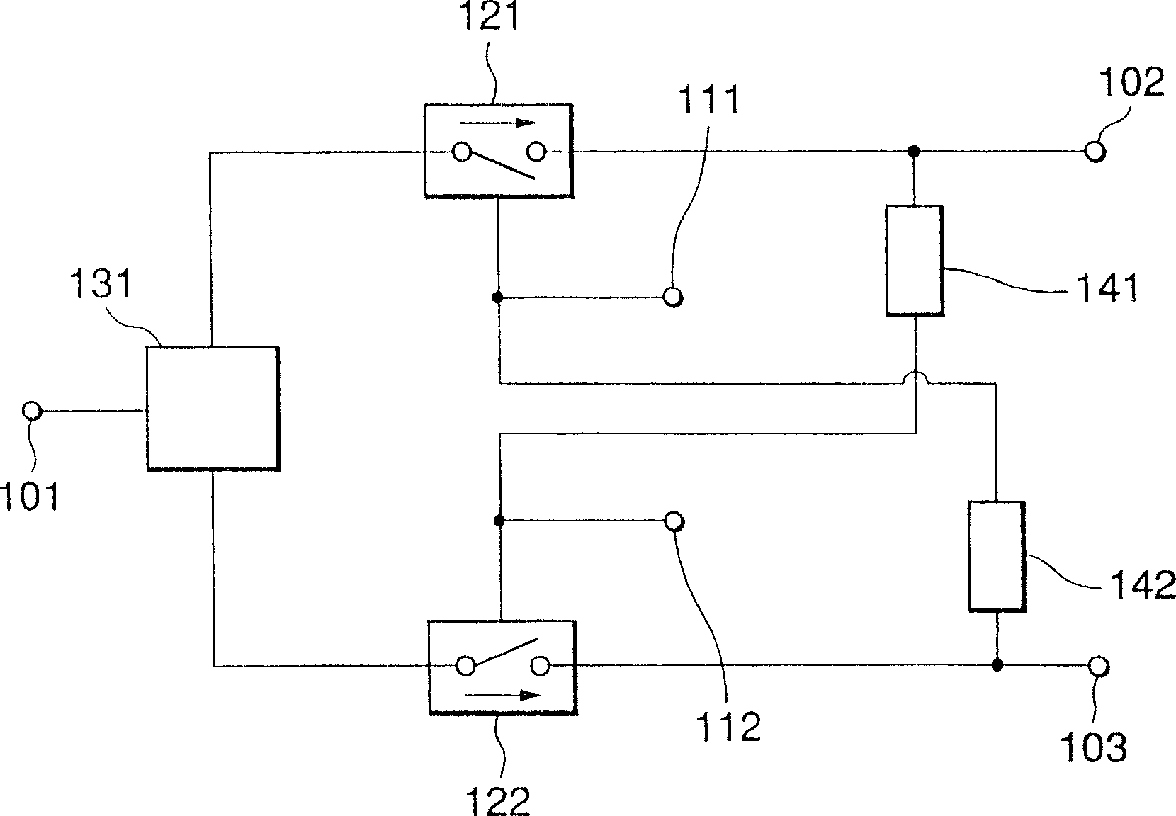
[0058] image 3 is a circuit diagram showing a first embodiment of the high-frequency switching circuit according to the present invention. will refer to image 3 This first embodiment will be described.

[0059] The high-frequency switch circuit according to the first embodiment includes: high-frequency terminals 101, 102, and 103 that input / output high-frequency signals; a high-frequency semiconductor switch section 121 that switches between high-frequency terminals 101 and 102; A semiconductor switch section 122 which switches between the high-frequency terminals 101 and 103; a switch signal terminal 111 which controls the switching operation of the high-frequency semiconductor switch section 121; a switch signal terminal 112 which controls the switching operation of the high-frequency semiconductor switch section 122 ; DC potential isolation part 131, which is connected between high-frequency terminal 101 and high-frequency semiconductor switch parts 121 and 122, and iso...


PUM


Abstract

This invention relates to a high frequency switch circuit including a plurality of high frequency terminals (101, 102, 103) which input / output a high frequency signal, and a plurality of high frequency semiconductor switch sections (121, 122) which switch between these high frequency terminals. The plurality of high frequency semiconductor switch sections are isolated from each other in a DC state by a DC potential isolating section (131), and a DC potential opposite in level to a DC potential applied to a switching signal terminal (111, 112) arranged on the control side of each high frequency semiconductor switch section is applied to both or at least one of the input side and output side of each high frequency semiconductor switch section.

Description

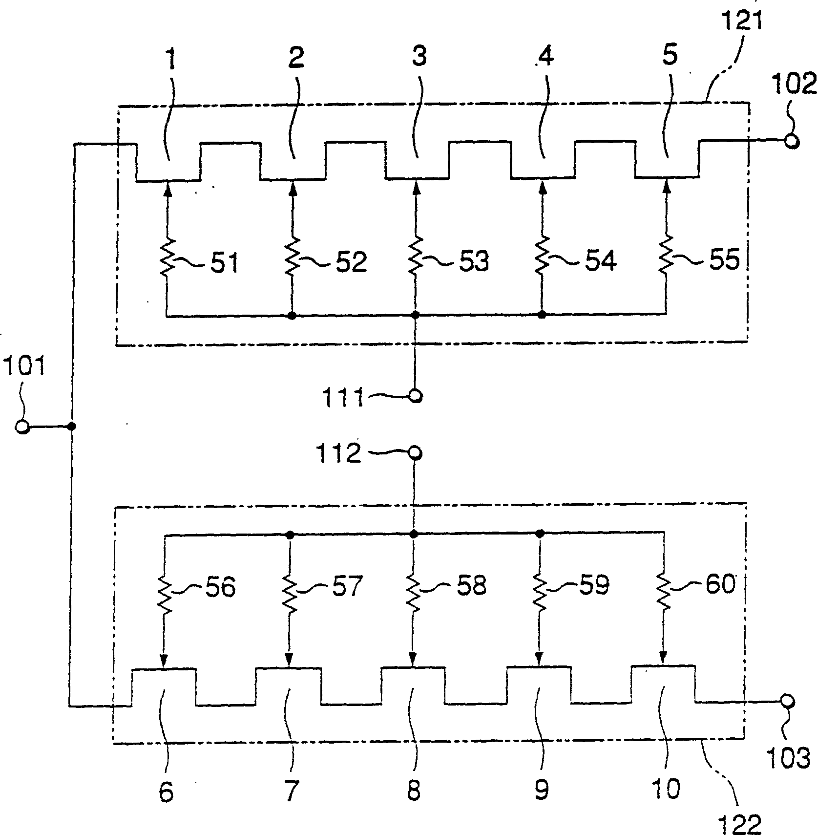
technical field [0001] The present invention relates to a high-frequency switching circuit used for high-frequency communication in portable cellular phone devices and the like. Background technique [0002] figure 1 is a circuit diagram showing a first prior art of a high-frequency switching circuit. This first prior art will refer to figure 1 illustrate. [0003] The first prior art relates to an SPDT circuit (Single Pole Double Transfer: Single Pole Double Throw), which is disclosed in Japanese Unexamined Patent Publication No. 8-139014. The drains and sources of field effect transistors 1 to 5 are cascade-connected between high frequency terminals 101 and 102 . The drains and sources of the field effect transistors 6 to 10 are cascaded between the high frequency terminal 101 and the high frequency terminal 103 . The gates of the field effect transistors 1 to 10 are connected to the resistance elements 51 to 60 . The resistance elements 51 to 55 connected to the gat...

Claims


Application Information

Patent Timeline
Patent Type & Authority Patents(China)
IPC IPC(8): H03K17/693H01P1/15H03K17/06H03K17/62
CPCH01P1/15H03K17/693H03K17/00
Inventor 沼田圭市
Owner NEC CORP
Learn More