CMOS I/O offset control circuit
A bias control and circuit technology, applied in control/regulation systems, electrical components, electronic switches, etc., can solve problems such as low anti-power interference rate
- Summary
- Abstract
- Description
- Claims
- Application Information
AI Technical Summary
Problems solved by technology
Method used
Image

Examples
Embodiment Construction
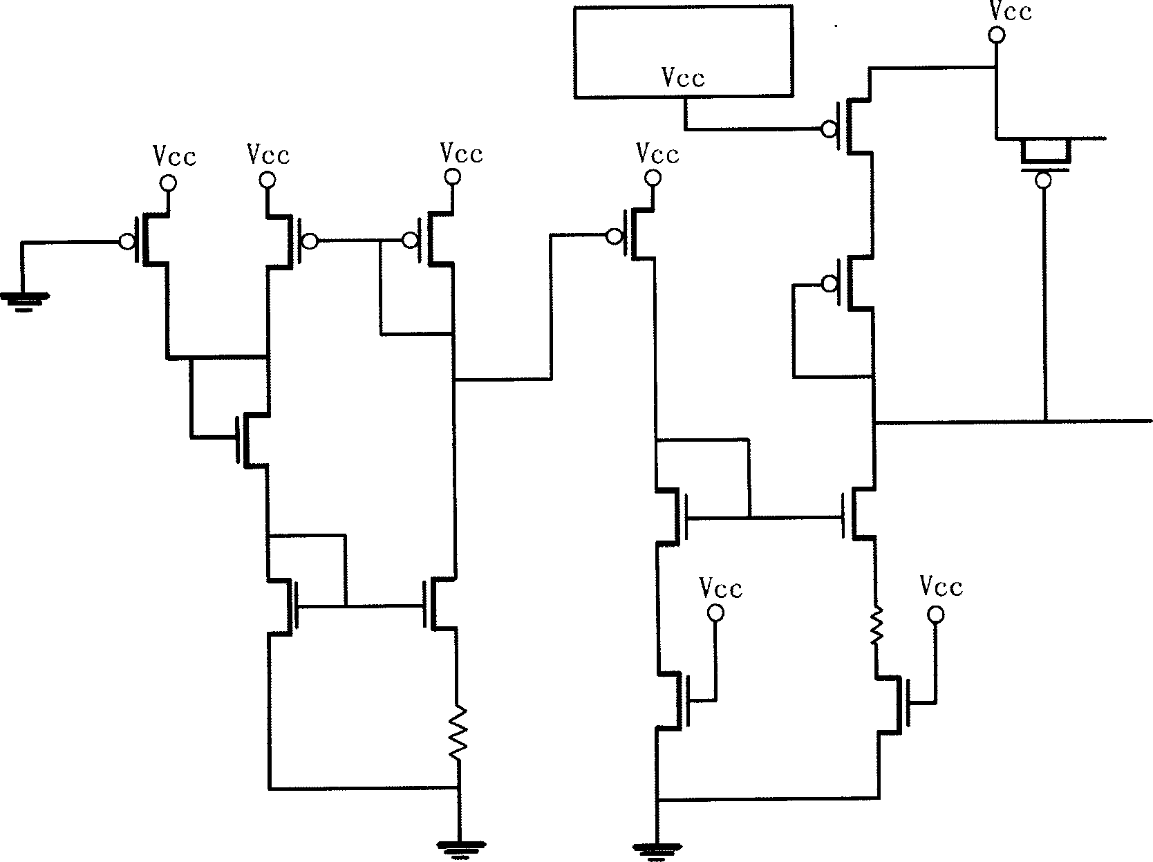
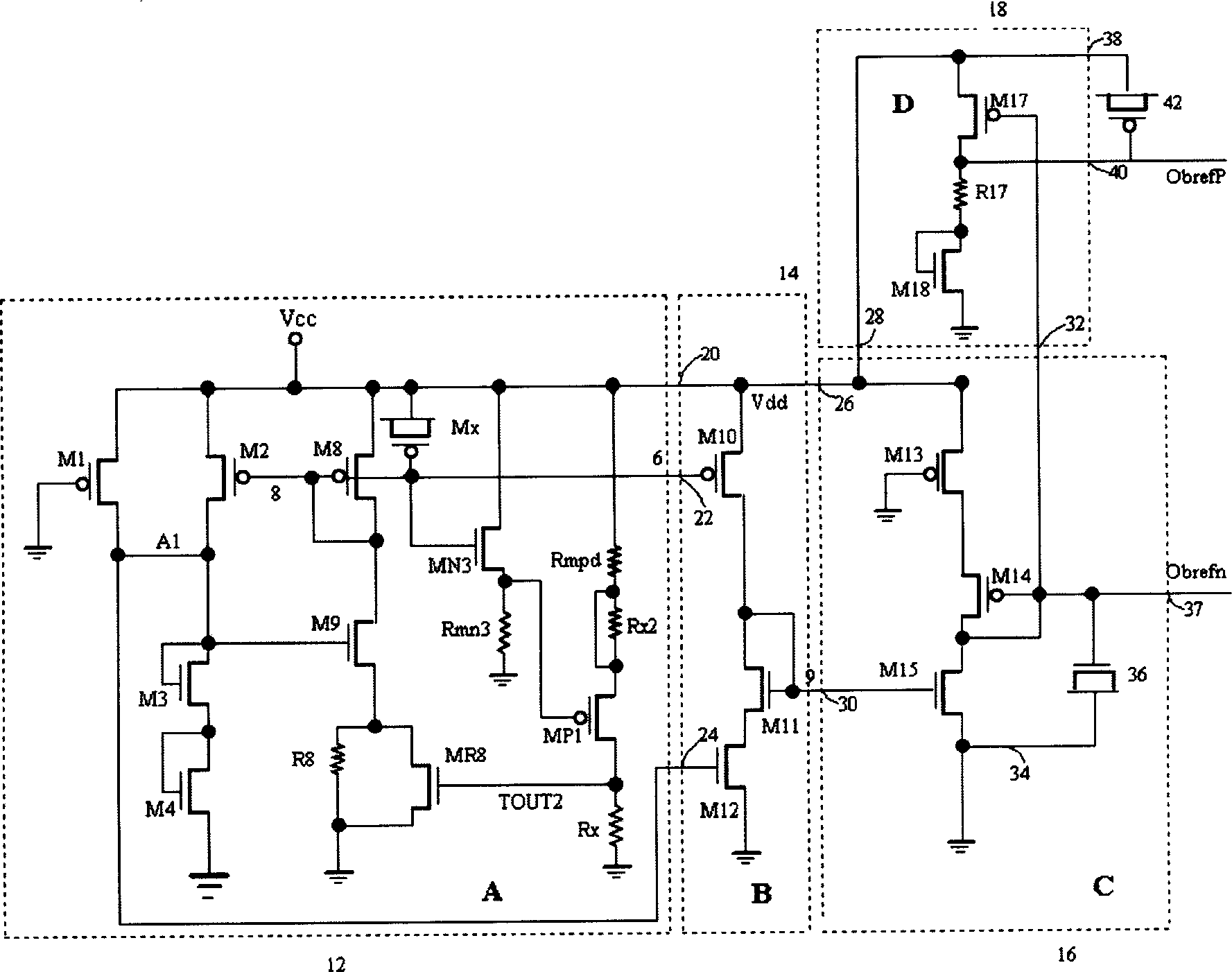
[0050] refer to figure 2 The circuit 10 shown specifically embodies the circuit connection relationship of the present invention. The circuit 10 is composed of four parts: a basic current source 12 , a first amplifier 14 , a second amplifier 16 and a third amplifier 18 . The source of the transistor M1, the source of the transistor M2, the source of the transistor M8, the source of the transistor MN3 and the first terminal of the resistor Rmpd are all connected to the input voltage Vcc. An input voltage Vcc is also present at the input 20 of the first amplifier 14 . The gate of transistor M1 is grounded. The gate of transistor M2 is connected to the gate and drain of transistor M8 and also to the drain of transistor M9. Transistor M9 is used to form the feedback path TOUT2. The feedback path TOUT2 improves the temperature and working process performance of the current source, making the output more stable and constant.
[0051] The drain of transistor M2 is connected to t...
PUM
 Abstract
Description
Claims
Application Information