
Micro image technique in use for encoding and arranging mask type ROM

A read-only memory and photolithography technology, applied in the field of photolithography, can solve the problems of increasing the difficulty and manufacturing cost of reticle, time-consuming reticle production, and difficulty in improving reticle pattern, so as to avoid deviation and reduce manufacturing. cost effect

Inactive Publication Date: 2006-10-18
MACRONIX INT CO LTD
View PDF0 Cites 0 Cited by
  • Summary
  • Abstract
  • Description
  • Claims
  • Application Information

AI Technical Summary

Problems solved by technology

However, this method must design a mask with a special pattern
Therefore, in addition to the time-consuming production of the reticle, it also increases the difficulty and cost of manufacturing the reticle.
In addition, after the mask plate is manufactured, it is extremely difficult to improve the defect of the mask plate pattern (Debug)

Method used


Image

  • Micro image technique in use for encoding and arranging mask type ROM
  • Micro image technique in use for encoding and arranging mask type ROM
  • Micro image technique in use for encoding and arranging mask type ROM

Examples


Embodiment Construction

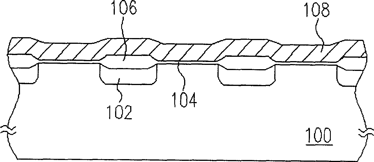
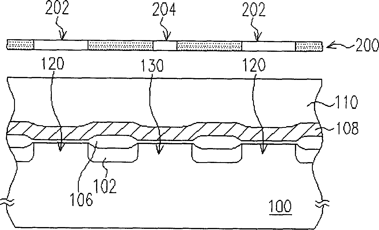
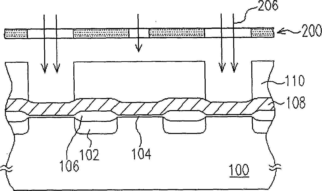
[0022] Figure 1A to Figure 1D As shown, it is a schematic cross-sectional flow diagram of the code implantation process of the mask-mode ROM according to a preferred embodiment of the present invention.

[0023] Please refer to Figure 1A , a mask mode read-only memory is composed of a plurality of memory cells arranged in a matrix, which includes a plurality of buried bit lines 102 disposed in the substrate 100, and a plurality of polysilicon word lines 108 across the bit lines 102 . The word line 108 is electrically isolated from the buried bit line 102 and the substrate 100 by an insulating structure 106 and a gate oxide layer 104 . Wherein, the region below the word line 108 and between two adjacent buried bit lines 102 is the channel region of the memory cell.

[0024] Next, a code implantation process is used to program the masked ROM. Its details are as follows.

[0025] Please refer to Figure 1B , forming a photoresist layer 110 on the substrate 100 to cover the...


PUM

PropertyMeasurementUnit
sizeaaaaaaaaaa
sizeaaaaaaaaaa
sizeaaaaaaaaaa

Abstract

A photolithography process applied to code implantation of a mask-mode read-only memory, which firstly provides a substrate, wherein a plurality of memory cells arranged in a matrix have been formed on the substrate. Next, a photoresist layer is formed on the substrate to cover the memory cells. Afterwards, a mask plate is set above the photoresist layer, wherein the mask plate has a plurality of code openings and a plurality of dummy openings, and the code openings correspond to a predetermined code implanted channel region, and the dummy openings correspond to the remaining The channel region, and the size of the dummy opening is smaller than a specific size, so that the dummy opening cannot be transferred to the photoresist layer in the subsequent photolithography process. Then, a photolithography process is performed to transfer the coding openings on the mask plate to the photoresist layer.

Description

technical field [0001] The present invention relates to a photolithography process (Photolithography), and in particular to a photolithography process applied to masked ROM code implantation (Code Implantation). Background technique [0002] A general structure of a masked ROM includes several bit lines (Bit Line, BL) and several polysilicon word lines (Word Line, WL) across the bit lines. The area below the word line and between two adjacent bit lines is the channel area of ​​the memory cell. For some mask-mode ROMs, the programming method uses whether or not ions are implanted in the channel to store data "0" or "1". The process of implanting ions in specific channel regions is also called code implantation process. [0003] Generally, in the code implantation process of the masked ROM, a mask plate is used to pattern the photoresist layer formed on the substrate to expose the channel region to be coded. Then, an ion implantation process is performed on the patterned ph...

Claims


Application Information

Patent Timeline
Patent Type & Authority Patents(China)
IPC IPC(8): H01L21/8246H01L21/027G03F7/00
Inventor 许伟华张庆裕钟维民
Owner MACRONIX INT CO LTD
Learn More