Layout structure of non-volatile memory

A non-volatile, layout structure technology, applied in information storage, static memory, read-only memory, etc., can solve the problems of short circuit, affecting the reliability of the process yield, poor process yield and reliability, etc., to save the process cost effect

Active Publication Date: 2007-12-26
MACRONIX INT CO LTD
View PDF0 Cites 0 Cited by
  • Summary
  • Abstract
  • Description
  • Claims
  • Application Information

AI Technical Summary

Problems solved by technology

[0003] Generally speaking, in the manufacturing process of the entire memory array, there are many variable factors, which will have a negative impact on the yield and reliability of the process.
For example, due to the limitations of the yellow light process, the components in the edge area of ​​the memory array will deviate from the critical dimension (Critical Dimension, CD) of the components in the center area (bias), which will directly or indirectly cause defects (such as leakage current, short circuit, etc.) etc.), affecting the yield and reliability of the process

Method used


Image

  • Layout structure of non-volatile memory
  • Layout structure of non-volatile memory

Examples


Embodiment Construction

[0040] In order to make the above and other objects, features and advantages of the present invention more comprehensible, preferred embodiments are described below in detail with accompanying drawings.

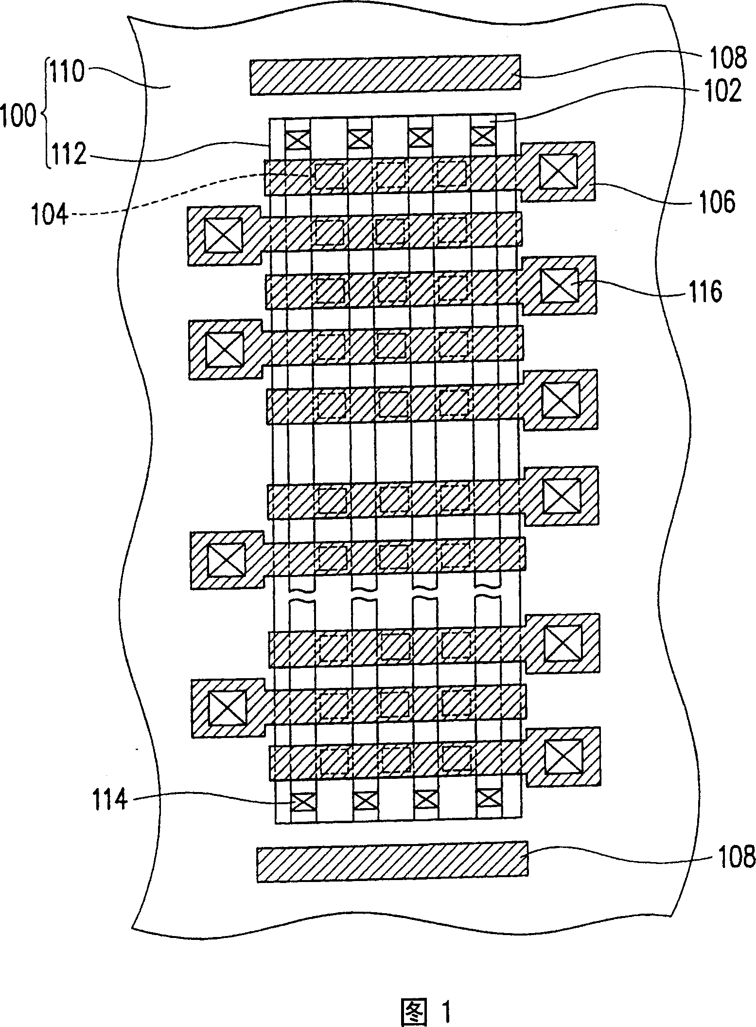
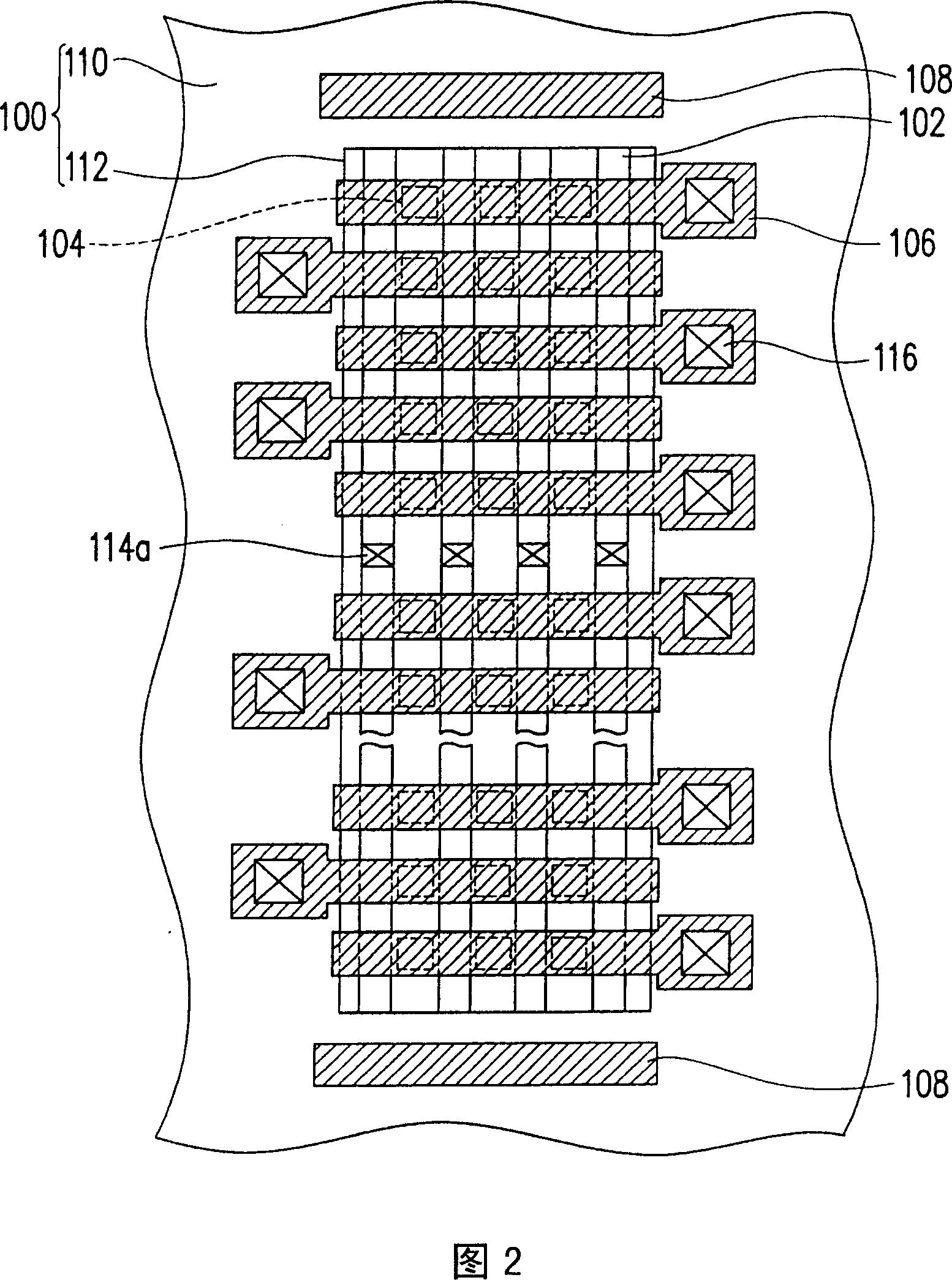
[0041] FIG. 1 is a top view of a layout structure of a non-volatile memory according to an embodiment of the present invention. There are 3 memory cells in each memory cell column in FIG. 1 , but the present invention is not limited thereto.

[0042] Please refer to FIG. 1, the layout structure of the non-volatile memory of the present embodiment mainly includes: a substrate 100, a plurality of buried bit lines (buried bit lines) 102 in the row direction, a plurality of transistors 104 as memory cells, and columns A plurality of word lines (word lines) 106 and dummy word lines (dummy word lines) 108 in the direction. Wherein, the row direction is generally perpendicular to the column direction. An isolation structure 110 is disposed in the substrate 100 to define an active ...


PUM


Abstract

The layout structure of non-volatile includes following parts: substrate; multiple flush type bit lines along row direction; multiple transistors as memory cells; multiple word lines along column direction, multiple contact windows of bit line; and at least two virtual word lines. Being located at the substrate, an isolation structure defines out drive region. Flush type bit lines are located at substrate of the drive region. Being setup at the substrate, transistors arranged in 2D array are located between flush type bit lines. Each word line is connected to each transistor in same column in series. Contact windows of bit line are located on flush type bit lines. Being parallel in word lines, two virtual word lines are positioned on the isolation structure at two sides of the drive region.

Description

technical field [0001] The present invention relates to a layout structure of a semiconductor component, and in particular to a layout structure of a non-volatile memory. Background technique [0002] With the rapid development of science and technology, when the functions of computer microprocessors become stronger and stronger, and the programs and calculations performed by software become larger and larger, the demand for memory becomes higher and higher, especially for the layout of memory components. The requirement for the accuracy of the layout rules, in order to meet the trend of manufacturing to meet this requirement, improving the technology of manufacturing memory components has become the driving force for the continuous challenge of semiconductor technology towards high integration. [0003] Generally speaking, there are many variable factors in the entire manufacturing process of the memory array, which will have a bad influence on the yield rate and reliabilit...

Claims


Application Information

Patent Timeline
Patent Type & Authority Applications(China)
IPC IPC(8): H01L27/105H01L27/115H01L23/528G11C11/56G11C16/02
Inventor 金钟五刘承杰
Owner MACRONIX INT CO LTD
Why Eureka
Try Eureka