Layout structure of non-volatile memory

A non-volatile, layout-structured technology, applied in information storage, static memory, read-only memory, etc., can solve problems such as short circuits, poor process yield and reliability, and affect process yield and reliability. The effect of saving process cost

Active Publication Date: 2009-08-05
MACRONIX INT CO LTD
View PDF3 Cites 0 Cited by
  • Summary
  • Abstract
  • Description
  • Claims
  • Application Information

AI Technical Summary

Problems solved by technology

[0003] Generally speaking, in the manufacturing process of the entire memory array, there are many variable factors, which will have a negative impact on the yield and reliability of the process.
For example, due to the limitation of the photolithography process, the critical dimension (Critical Dimension, CD) deviation (bias) between the components in the edge area of ​​the memory array and the components in the central area will occur, which will directly or indirectly cause defects (such as leakage current, short circuit, etc.) etc.), affecting the yield and reliability of the process

Method used


Image

  • Layout structure of non-volatile memory
  • Layout structure of non-volatile memory

Examples


Embodiment Construction

[0038] In order to make the above-mentioned and other objects, features and advantages of the present invention more obvious and easy to understand, the preferred embodiments are hereinafter described in detail together with the accompanying drawings.

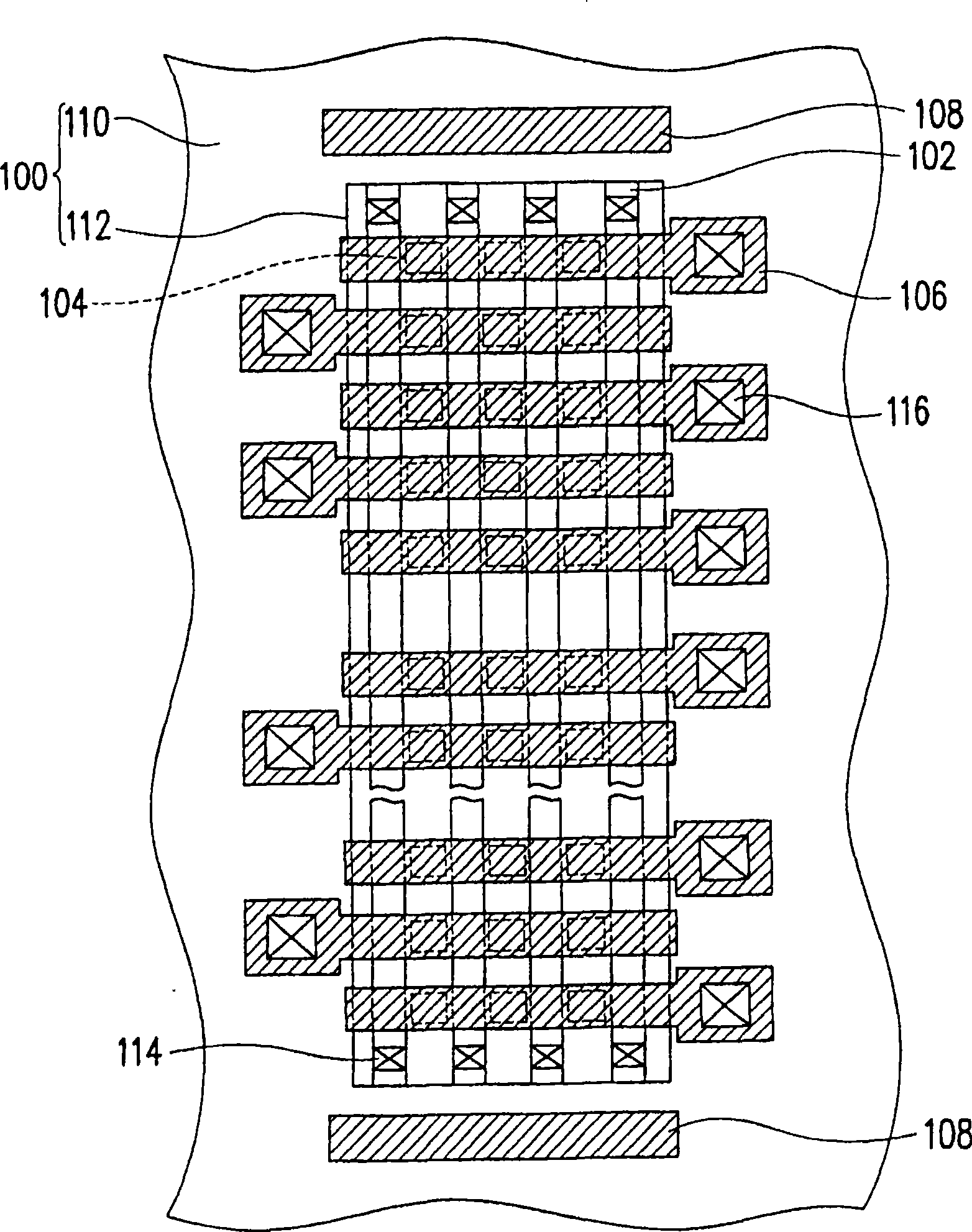
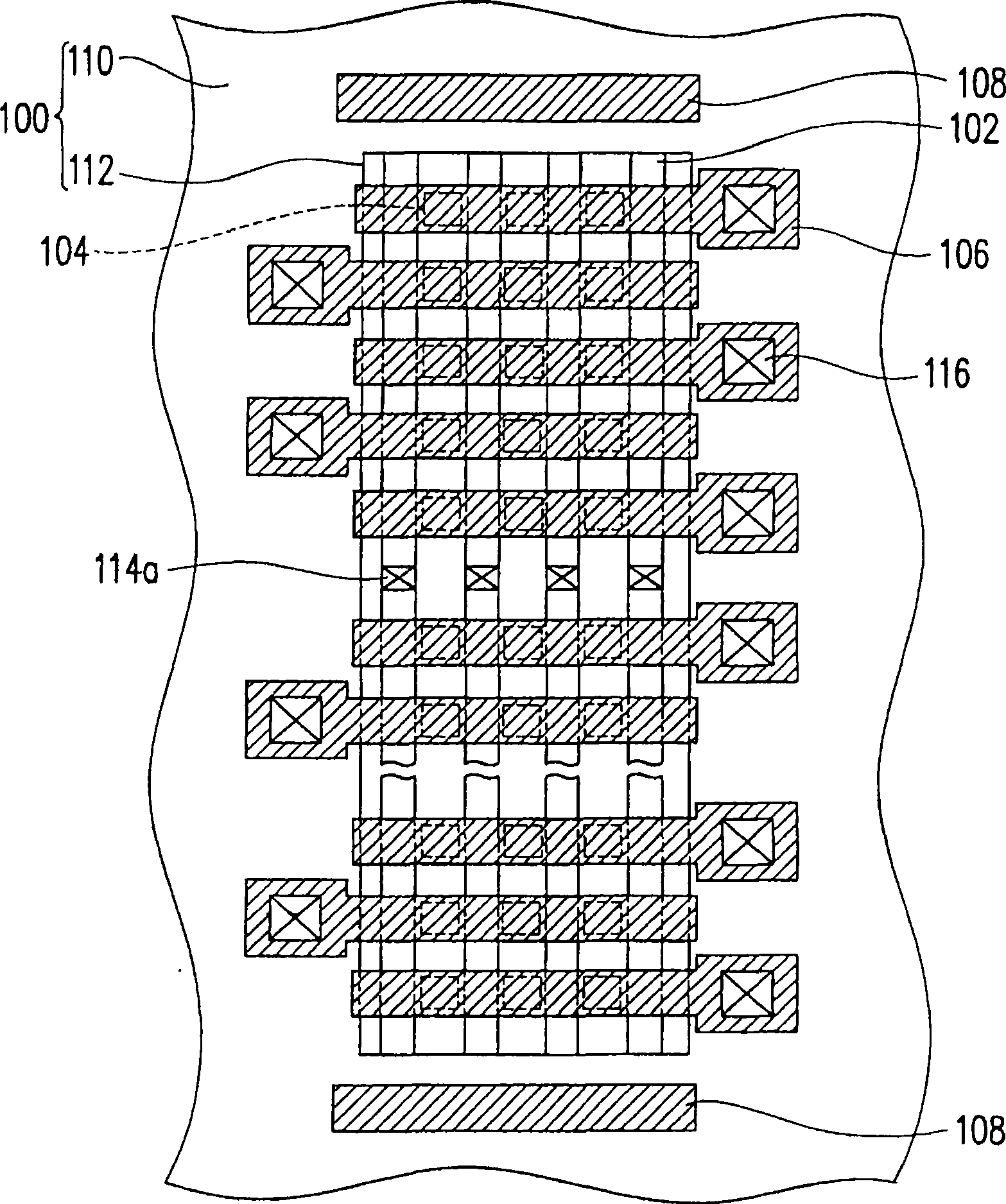
[0039] figure 1 It is a top view of a layout structure of a non-volatile memory according to an embodiment of the present invention. exist figure 1 There are 3 memory cells in each memory cell column, but the present invention is not limited to this.

[0040] Please refer to figure 1 The layout structure of the non-volatile memory in this embodiment mainly includes: a substrate 100, a plurality of buried bit lines 102 in a row direction, a plurality of transistors 104 as memory cells, a plurality of A word line 106 and a dummy word line 108 are provided. Among them, the row direction is generally perpendicular to the column direction. An isolation structure 110 is formed in the substrate 100 to define an active region 112 ...


PUM


Abstract

A layout structure of a non-volatile memory, which includes: a substrate, a plurality of embedded bit lines in a row direction, a plurality of transistors as memory cells, a plurality of word lines in a column direction, a plurality of bit line contact windows and at least Two virtual character lines. There is an isolation structure in the substrate, and the isolation structure defines an active area. The buried bit line is located in the base of the active area. Transistors are located on the substrate between the buried bit lines and arranged in a two-dimensional array. Each word line connects the transistors of the same column in series. The bitline contacts are located on the buried bitlines. In addition, the two dummy word lines are respectively located on the isolation structures on both sides of the active area, and are arranged parallel to the word lines.

Description

technical field [0001] The present invention relates to a layout structure of a semiconductor device, and more particularly, to a layout structure of a non-volatile memory. Background technique [0002] With the rapid development of science and technology, when the functions of computer microprocessors are getting stronger and stronger, and the programs and operations performed by software are getting larger and larger, the demand for memory is also getting higher and higher, especially regarding the layout of memory components. The requirement for the accuracy of layout rules, and in order to manufacture to meet this demand trend, improving the technology of making memory devices has become the driving force behind the continuous challenge of high integration in semiconductor technology. [0003] Generally speaking, in the manufacturing process of the entire memory array, there are many variation factors, which will adversely affect the yield and reliability of the process....

Claims


Application Information

Patent Timeline
Patent Type & Authority Patents(China)
IPC IPC(8): H01L27/105H01L27/115H01L23/528G11C11/56G11C16/02
Inventor 金钟五刘承杰
Owner MACRONIX INT CO LTD
Why Eureka
Try Eureka