Circuit board design method

A design method and circuit board technology, applied in printed circuit, multi-layer circuit manufacturing, printed circuit manufacturing, etc., can solve problems such as integrity and impedance not meeting requirements, increasing circuit board cost, circuit signal reference plane damage, etc., to achieve Increase design difficulty, ensure signal quality, and reduce cost

Inactive Publication Date: 2003-08-20
惠州中京电子科技股份有限公司
View PDF0 Cites 9 Cited by
  • Summary
  • Abstract
  • Description
  • Claims
  • Application Information

AI Technical Summary

Problems solved by technology

[0004] In the existing circuit board design method, the reference plane can only be used as a strict power supply or ground plane, and the wiring cannot be routed on the reference plane. If the wiring is routed on the reference plane, the following two problems will occur: one is the original signal layer. The reference plane of the circuit signal is destroyed, and its integrity and impedance may not meet the requirements; second, for the wiring on the reference plane, both sides of the layer are previous signal layers, and there is no reference plane at all. It is not guaranteed, and it will also introduce radiation and interference into the original reference plane power and ground
Therefore, in the existing circuit board design, if there are a small number of signal lines that cannot be routed on the predetermined signal layer, the wiring layer can only be added to the circuit board. Of course, the corresponding reference plane must also be increased, thereby increasing the number of circuit boards. cost

Method used


Image

  • Circuit board design method
  • Circuit board design method
  • Circuit board design method

Examples


Embodiment Construction

[0016] The present invention will be further described in detail below in conjunction with the accompanying drawings and embodiments.

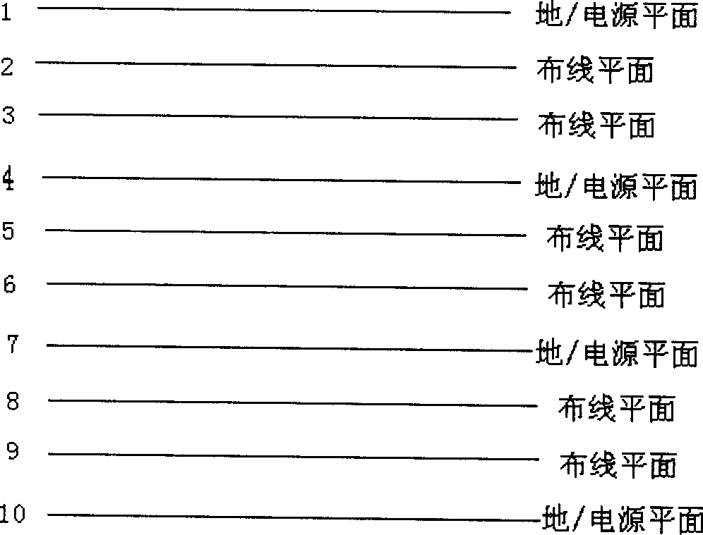
[0017] The essence of the present invention is to adopt copper cladding technology for the reference plane layer and the wiring layer of the circuit board, so that a small amount of wiring can be added to the reference plane layer, and the wiring of the wiring layer and the reference plane layer have reference planes.

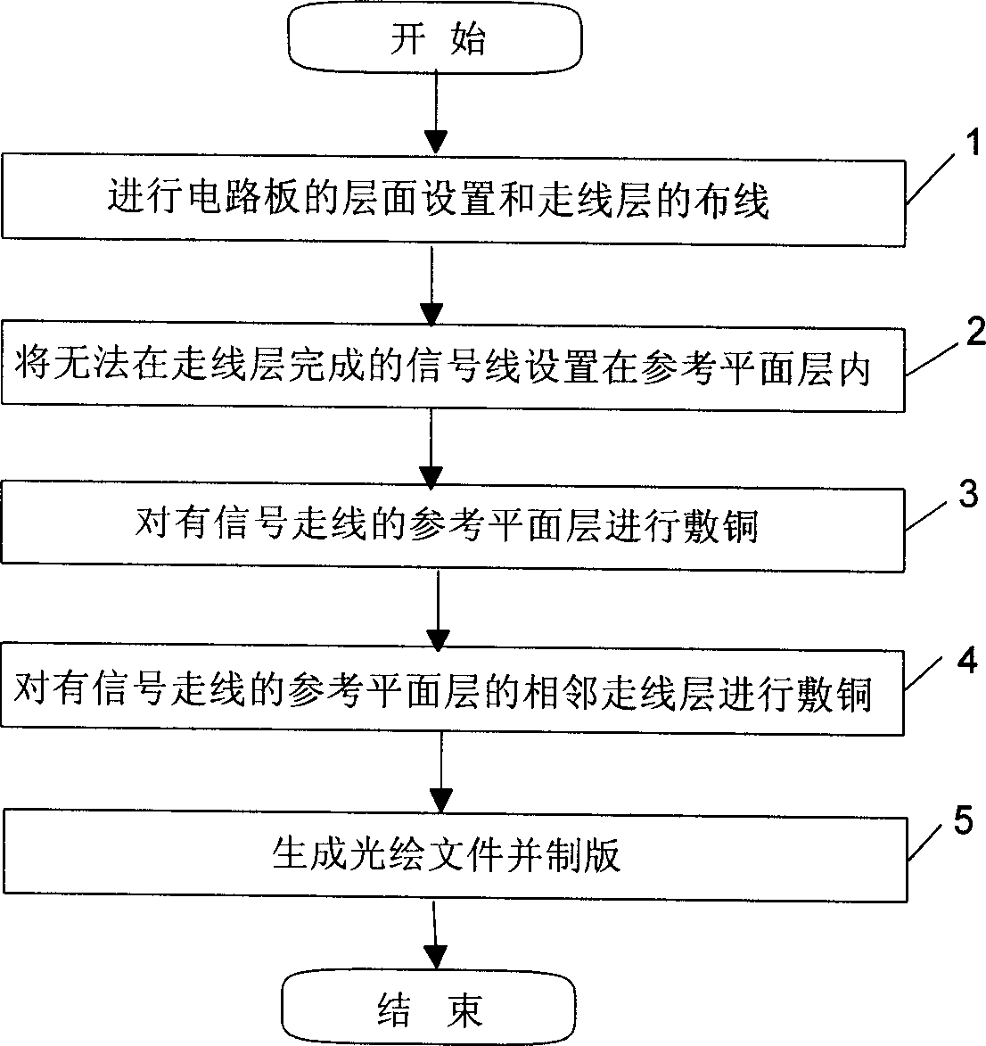
[0018] figure 1 It is the flow chart of the embodiment of the method of the present invention, to figure 1 References for understanding the method figure 2 . according to figure 1 , firstly, in the first step, complete the layer setting of the circuit board and the wiring setting of the wiring layer according to the usual circuit board design requirements, and divide the signal wiring that cannot be completed in the predetermined wiring layer. In step 2, the routing that cannot be completed on the predetermined routing lay...


PUM


Abstract

A design method of circuit board carries on surface set-up of the circuit board and wiring set-up of routing layer first and divided out the signal routing which can not be finished at routing layer but to be finished in reference plane layer where should be carried on with copper cladding that its nature should be keps as original nature of the reference plane layer. The routing layer adjacent to the reference plane layer set with signal routing will also be cladded with copper. Which has its nature as "earth" and at least the optical plotting file will be produced as well as platemaking of the circuit board should be carried on according to the produced file.

Description

technical field [0001] The invention relates to a design method of a circuit board in an electronic device. Background technique [0002] In the circuit board design of existing communication equipment and high-speed measurement equipment, the signal integrity and electromagnetic compatibility (EMC) performance requirements are getting higher and higher, the signal density is getting higher and higher, and the design cost requirements are getting lower and lower. , this requires that in the design of the circuit board, on the one hand, it is necessary to meet the requirements of a good reference plane for signal routing, and on the other hand, it is necessary to minimize the number of design layers of the circuit board and reduce the cost of circuit board design. However, it is difficult to unify the above-mentioned contradictions by adopting the existing circuit board design method. For example, in the backplane design of communication equipment, the backplane signals have...

Claims


Application Information

Patent Timeline
IPC IPC(8): H05K3/00H05K3/10H05K3/46
Inventor 邱隆
Owner 惠州中京电子科技股份有限公司
Why Eureka
Try Eureka