

Semiconductor device
A technology for semiconductors and devices, applied in the field of resin-sealed semiconductor devices, can solve the problems of large differences in resin filling and other problems
- Summary
- Abstract
- Description
- Claims
- Application Information
AI Technical Summary
Problems solved by technology
Method used
Image



Examples
Embodiment Construction
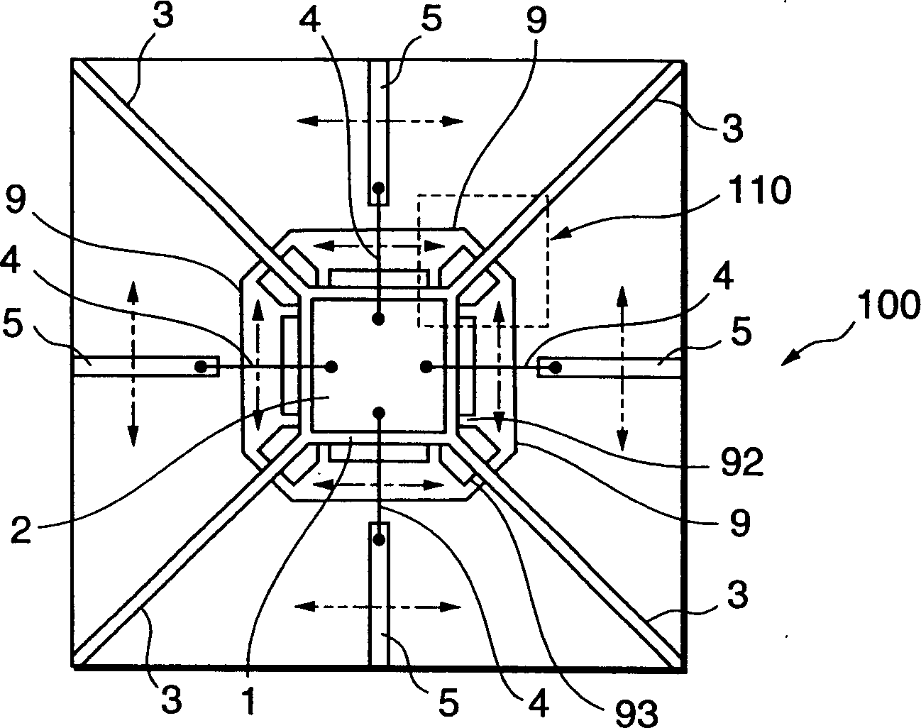
[0026] The present invention will be described below with reference to the accompanying drawings. 1 is a view describing a semiconductor device of an embodiment of the present invention, in a state where a semiconductor chip is mounted on a lead frame, and electrodes of the semiconductor chip and edge portions of internal leads are connected by bonding wires, wherein Figure 1A is the floor plan, Figure 1B yes Figure 1A The enlarged floor plan of the part 110 indicated by the dotted line in . The other three hanger leads and their peripheral parts have the same structure.
[0027] 2 is a view describing an inner lead of a lead frame and a peripheral portion thereof of an embodiment of the present invention, wherein, Figure 2A is the floor plan, Figure 2B yes Figure 2A An enlarged plan view of the portion 120 indicated by the middle dotted line. The other three hanger leads and their peripheral parts have the same structure.
[0028] In the figure, four hanger leads...
PUM
 Abstract
Description
Claims
Application Information