Chip packaging structure

A chip packaging structure and chip technology, applied in the direction of electrical components, electrical solid devices, circuits, etc., can solve the problem of high cost and achieve the effect of reducing packaging costs

Inactive Publication Date: 2003-12-17
ASE ASSEMBLY & TEST SHANGHAI
View PDF1 Cites 5 Cited by
  • Summary
  • Abstract
  • Description
  • Claims
  • Application Information

AI Technical Summary

Problems solved by technology

Therefore, this traditional packaging structure has the disadvantage of high cost

Method used


Image

  • Chip packaging structure
  • Chip packaging structure
  • Chip packaging structure

Examples


Embodiment Construction

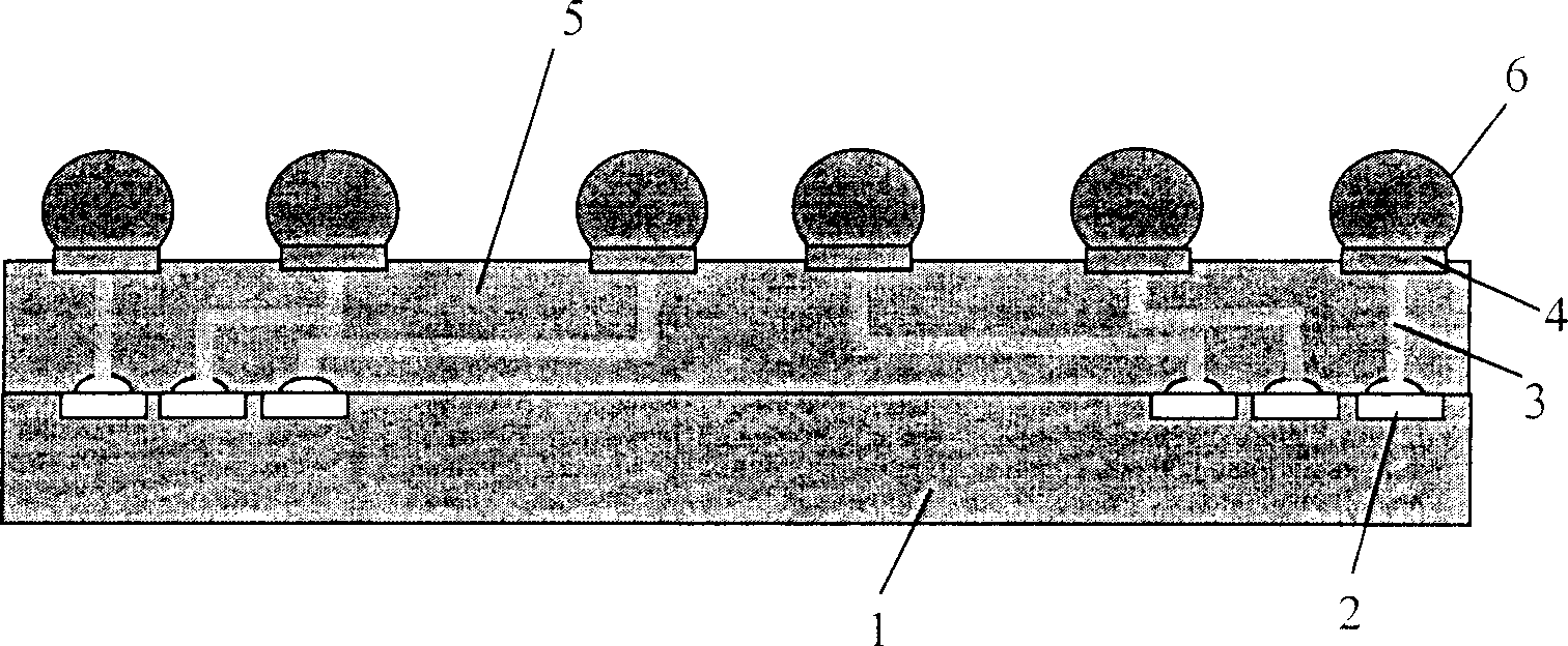
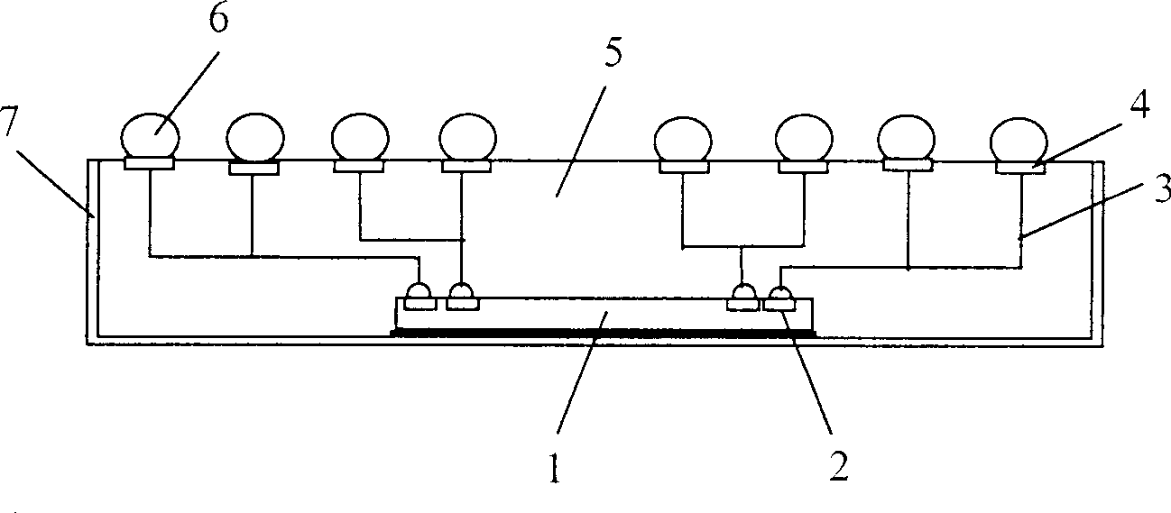
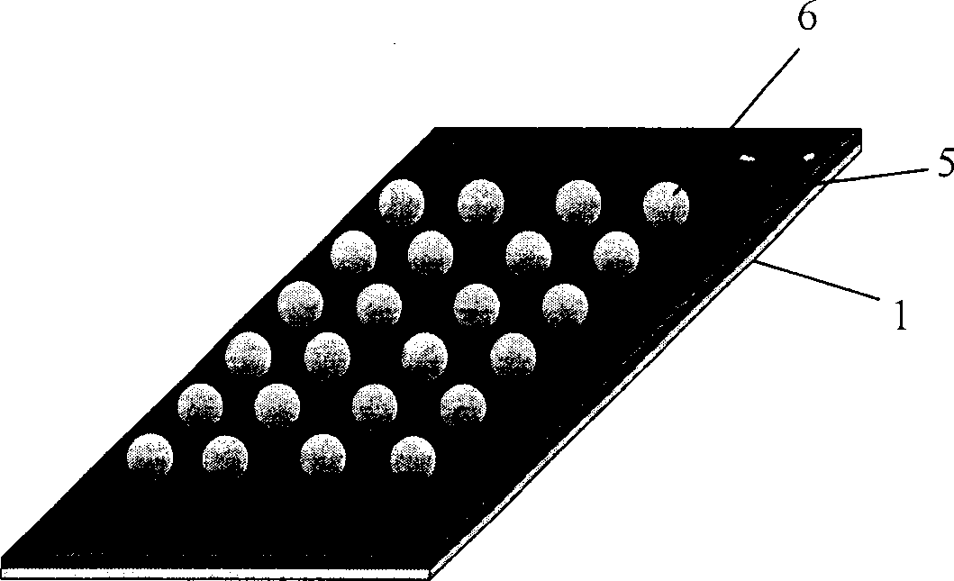
[0017] Such as figure 1 as shown, figure 1 A schematic diagram of the internal structure of the improved chip packaging structure of the present invention is shown. Please refer to figure 1 In the figure, 1 is a chip to be packaged. On the upper surface of the chip 1, there is a lead pad 2. The lead pad 2 is electrically connected to the pad 4 on the same side of the chip through a metal connection wire 3. The metal connecting wire 3 between the pad 2 and the pad 2 is filled with a filler 5, and the filler 5 is generally made of an insulating material, such as a polymer such as epoxy resin or thermosetting resin. Solder balls 6 are welded on the pads 4 by conventional techniques, thereby completing the packaging process of the chip.

[0018] The chip package structure of the present invention and Figure 4 and 5 Compared with the traditional chip packaging structure shown, the substrate is omitted, and the wiring method of the chip is simplified, so the cost of chip pac...


PUM


Abstract

A package structure without substrate for chip is composed of chip and the weld balls welded onto pads, and features that said weld balls are positioned on the one chip surface where the pads for leading wires are positioned, said pads are connected to the pads for leading wires on chip via metal wires, and the filler is filled between metal wires. Its advantage is low cost caused by omitting substrate.

Description

technical field [0001] The invention relates to a package structure of a chip, in particular to a package structure of a chip directly packaged without a substrate part. Background technique [0002] In the existing semiconductor packaging technology, there is a well-known ball grid array (BGA) packaging method. For example, US Patent No. 5,216,278 discloses this technology, which provides a high-pin device an effective solution. [0003] Refer below Figure 4 and Figure 5 This known encapsulation method is briefly described. Figure 4 is a schematic diagram of the appearance of a traditional ball grid array package structure; Figure 5 is a schematic cross-sectional view of a conventional ball grid array package structure. Such as Figure 4 and 5 As shown, this package structure includes a substrate 101 and a semiconductor chip 102 , and the semiconductor chip 102 is usually fixed on the surface of the substrate 101 by an adhesive 103 during manufacture. The chip 102 ...

Claims


Application Information

Patent Timeline
Patent Type & Authority Applications(China)
IPC IPC(8): H01L23/29H01L23/48
CPCH01L24/19H01L2224/19H01L2224/48091H01L2224/73265H01L2924/15311H01L2924/00014H01L2924/00012
Inventor 李铭训
Owner ASE ASSEMBLY & TEST SHANGHAI
Why Eureka
Try Eureka