Photoelectric sensor packaging structure

A photoelectric sensor and packaging structure technology, applied in circuits, electrical components, semiconductor devices, etc., can solve problems such as affecting the maintenance efficiency of photoelectric sensors, time-consuming and labor-intensive disassembly and replacement, etc.

Inactive Publication Date: 2021-03-19
西安远讯光电科技有限公司
View PDF0 Cites 4 Cited by
  • Summary
  • Abstract
  • Description
  • Claims
  • Application Information

AI Technical Summary

Problems solved by technology

[0003] In the prior art, the photoelectric sensor is an integral structure that cannot be disassembled after packaging. When the internal chip fail

Method used


Image

  • Photoelectric sensor packaging structure
  • Photoelectric sensor packaging structure
  • Photoelectric sensor packaging structure

Examples


Embodiment Construction

[0020] The following will clearly and completely describe the technical solutions in the embodiments of the present invention with reference to the accompanying drawings in the embodiments of the present invention. Obviously, the described embodiments are only some, not all, embodiments of the present invention.

[0021] In describing the present invention, it should be understood that the terms "upper", "lower", "front", "rear", "left", "right", "top", "bottom", "inner", " The orientation or positional relationship indicated by "outside", etc. is based on the orientation or positional relationship shown in the drawings, and is only for the convenience of describing the present invention and simplifying the description, rather than indicating or implying that the referred device or element must have a specific orientation, so as to Specific orientation configurations and operations, therefore, are not to be construed as limitations on the invention.

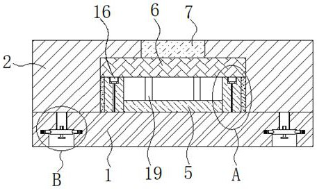
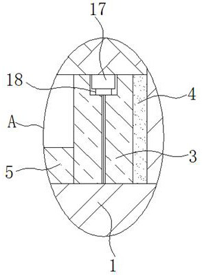
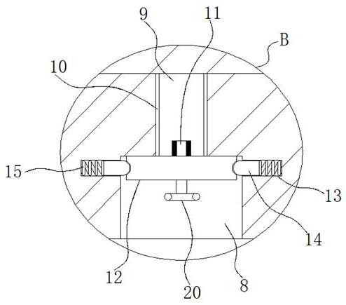
[0022] refer to Figure ...


PUM


Abstract

The invention relates to the technical field of sensor packaging, and discloses a photoelectric sensor packaging structure. The structure comprises a substrate and a packaging plate, the upper surfaceof the substrate is attached to the lower surface of the packaging plate, a frame body is fixedly connected to the upper surface of the substrate, a groove corresponding to the frame body is formed in the lower surface of the packaging plate, the frame body and the groove are arranged in a clamped mode, ,a matched sealing strip is installed at the joint of the frame body and the groove, a matchedcontrol processing chip is arranged in the frame body and electrically connected with the substrate, a matched photoelectric sensor chip is arranged at the groove bottom of the groove, the lower surface of the photoelectric sensor chip is attached to the top of the frame body, an opening is formed in the groove bottom of the groove and matched glass is fixedly mounted in the opening. According tothe invention, the packaging effect of the photoelectric sensor can be effectively ensured, the packaged photoelectric sensor can be conveniently maintained as required, and the maintenance efficiency is effectively ensured.

Description

technical field [0001] The invention relates to the technical field of sensor packaging, in particular to a photoelectric sensor packaging structure. Background technique [0002] A photoelectric sensor is a device that converts light signals into electrical signals. Its working principle is based on the photoelectric effect. The photoelectric effect refers to that when light is irradiated on certain substances, the electrons of the substance absorb the energy of photons and a corresponding electric effect occurs. [0003] In the prior art, the photoelectric sensor is an inseparable monolithic structure after packaging. When the internal chip breaks down and requires maintenance, it takes time and effort to dismantle and replace it, which greatly affects the maintenance efficiency of the photoelectric sensor. Contents of the invention [0004] The purpose of the present invention is to solve the above problems in the background technology, and propose a photoelectric sen...

Claims


Application Information

Patent Timeline
IPC IPC(8): H01L31/0203H01L31/02
CPCH01L31/02019H01L31/0203
Inventor 孙博郑波李浩
Owner 西安远讯光电科技有限公司
Why Eureka
Try Eureka