
Structure of double-bit cover screen type only-read memory and its making method

A technology of read-only memory and manufacturing method, which is applied in semiconductor/solid-state device manufacturing, electric solid-state devices, semiconductor devices, etc., and can solve problems such as memory unit interference, easy second-bit effect, and small operating margin, so as to avoid Effects of mutual interference, elimination of second place effect, and improvement of operating margin

Inactive Publication Date: 2004-02-25
MACRONIX INT CO LTD
View PDF0 Cites 1 Cited by
  • Summary
  • Abstract
  • Description
  • Claims
  • Application Information

AI Technical Summary

Problems solved by technology

[0009] However, since the buried drain junction of the known dual-bit mask ROM is connected to the dual-bit code region, junction leakage is very likely to occur, and the second Second Bit Effect
In addition, there is still a problem in the known dual-bit mask ROM, that is, the memory cells in the memory element are easily interfered by other memory cells around them.
And because the storage unit of the known double-bit mask ROM is easily disturbed by other surrounding storage units and is prone to cause the second bit effect, the operating margin (OperationWindow) of the known memory element is relatively small.

Method used


Image

  • Structure of double-bit cover screen type only-read memory and its making method
  • Structure of double-bit cover screen type only-read memory and its making method
  • Structure of double-bit cover screen type only-read memory and its making method

Examples


Embodiment Construction

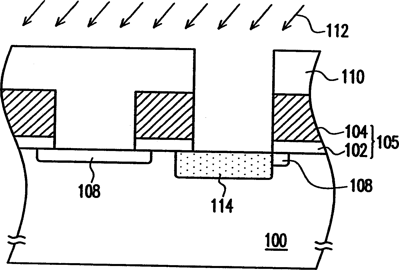
[0027] Figure 2A to Figure 2E , which is a schematic cross-sectional view of the manufacturing process of the dual-bit mask ROM according to a preferred embodiment of the present invention.

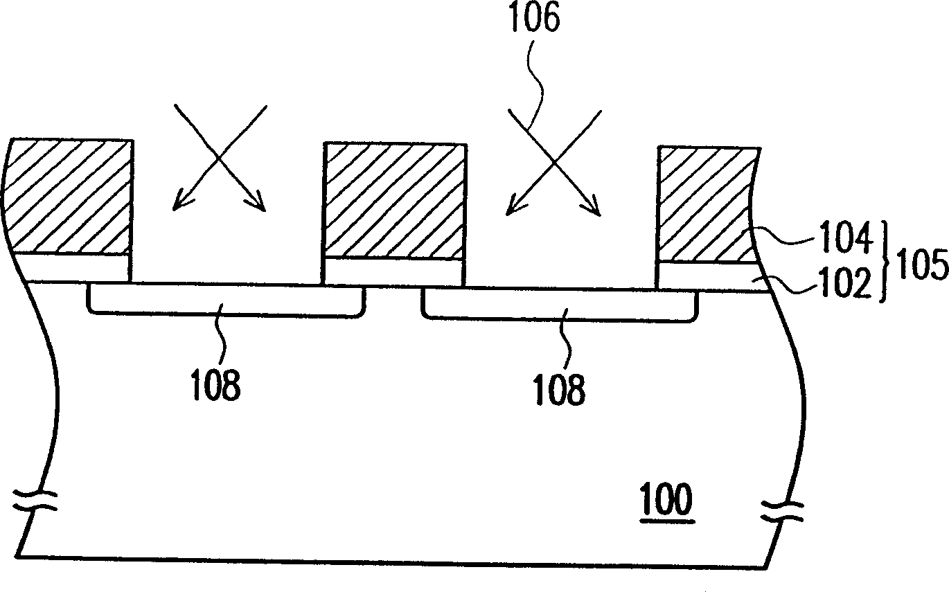
[0028] Please refer to Figure 2A Firstly, a gate structure 105 is formed on a substrate 100 . Wherein, the gate structure 105 includes a gate conductive layer 104 and a gate oxide layer 102 formed under the gate conductive layer 104 . In this embodiment, the material of the gate conductive layer 104 is, for example, polysilicon, and the thickness of the gate oxide layer 102 is, for example, about 45 angstroms.

[0029] Next, a pocket-type ion implantation step 106 is performed to form a pocket-type doped region 108 in the substrate 100 on both sides of the gate structure 105 . In this embodiment, the ions implanted in the pocket-type doped region 108 are, for example, arsenic ions, and an ion implantation dose in the pocket-type ion implantation step 106 is, for example, 1×10 13 / cm...


PUM


Abstract

The present invention relates to a structure of dibit cover-curtain type read-only memory and its making method. The structure includes a substrate, a grid structure, a dibit coding region, a gap wall, an embedded drain, a doped regio, an insulating layer and a character line.

Description

technical field [0001] The present invention relates to a structure of a mask-type ROM and a manufacturing method thereof, in particular to a structure of a dual-bit mask-type ROM and a manufacturing method thereof. Background technique [0002] Masked ROM is the most basic type of ROM. It mainly adjusts its threshold voltage (Threshold Voltage) through an ion implantation process, so as to achieve the purpose of controlling the memory cell to be turned on (On) or turned off (Off). When the product of the mask-type read-only memory is changed, the process does not need to be greatly modified, but only a set of photomasks used is changed, so it is very suitable for mass production, and even a part of the process can be made first. For semi-finished products, when the order arrives at the factory, these semi-finished products can be quickly programmed (Programming), which can effectively shorten the delivery time. [0003] A dual-bit mask ROM is currently under active develo...

Claims


Application Information

Patent Timeline
Patent Type & Authority Applications(China)
IPC IPC(8): H10B20/00
Inventor 刘慕义范左鸿詹光阳叶彦宏卢道政
Owner MACRONIX INT CO LTD
Learn More