System and method for using dynamic random access memory and flash memory

A technology of random access memory and memory system, which is applied in the field of memory systems and can solve problems such as weakening SRAM compatibility

Inactive Publication Date: 2004-03-17
HITACHI LTD +1
View PDF2 Cites 8 Cited by
  • Summary
  • Abstract
  • Description
  • Claims
  • Application Information

AI Technical Summary

Problems solved by technology

Unfortunately, this read time impairs compatibility with SRAM

Method used


Image

  • System and method for using dynamic random access memory and flash memory
  • System and method for using dynamic random access memory and flash memory
  • System and method for using dynamic random access memory and flash memory

Examples


Embodiment 2

[0254] Figure 27A with 27B A second embodiment of a memory module suitable for use in the memory system of the present invention is shown. Figure 27A is the top view of the memory module, Figure 27B It is a sectional view formed along the line A-A' of the top view.

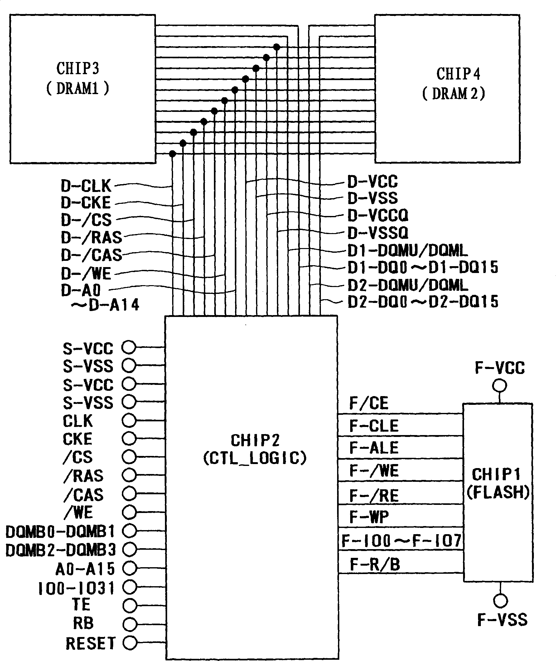
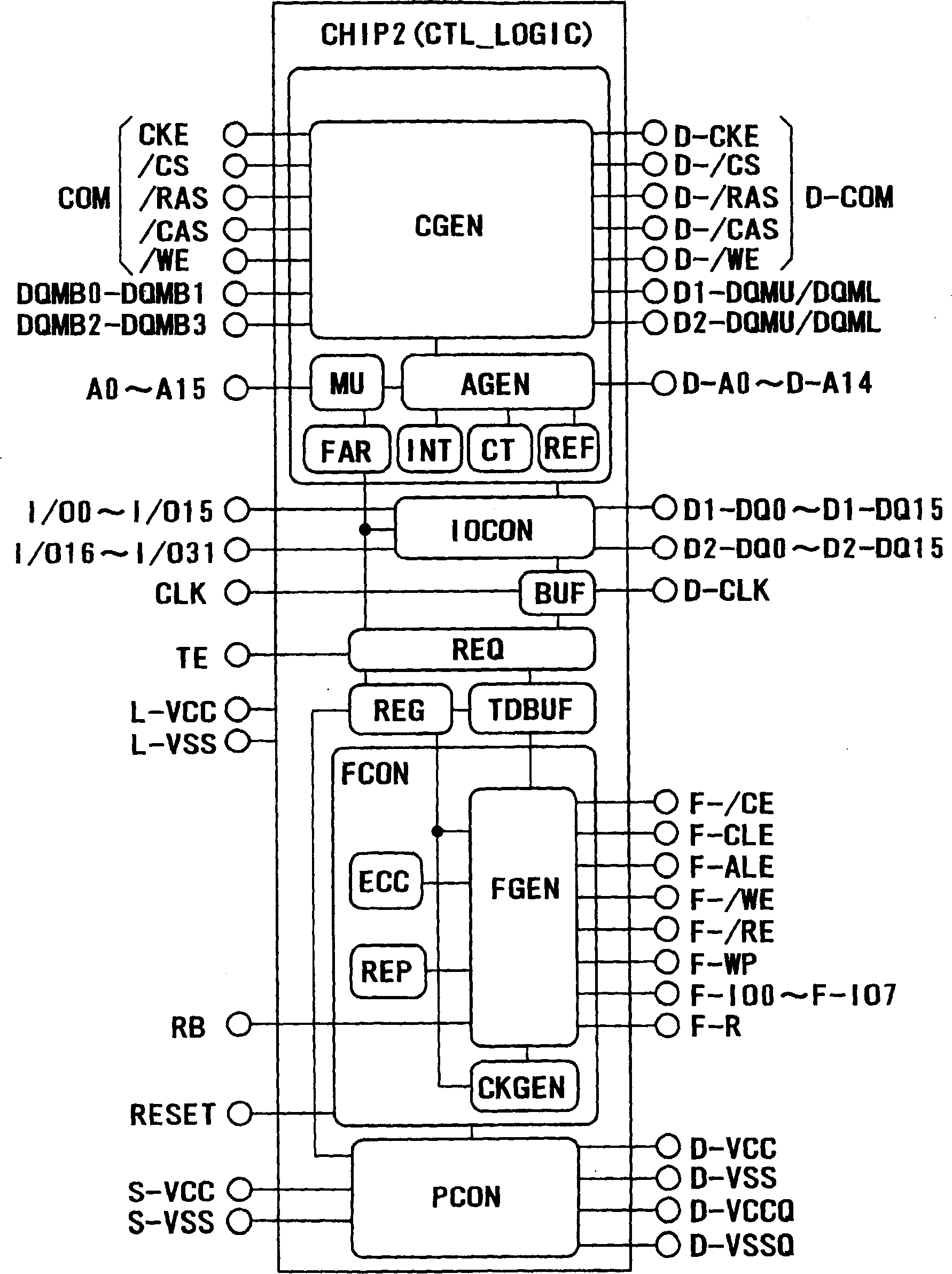
[0255] In the memory module of this embodiment, CHIP1 (FLASH), CHIP2 (CTL_LOGIC), CHIP3 (DRAM1) and CHIP4 (DRAM2) are mounted on a PCB board mounted on the device through a ball grid array (BGA) (for example, by a ring on a printed circuit board made of oxygen glass substrate). A bare chip of a general-purpose DRAM in which signal and power pads are arranged in rows in a so-called chip center is used for CHIP3 and CHIP4, but is not limited thereto. A bare chip of general-purpose FLASH in which signal and power pads are arranged in rows at one end of the so-called chip is used for CHIP1, but is not limited thereto.

[0256] The soldering point on CHIP1 and the soldering point on the PCB are connected to eac...

Embodiment 3

[0264] Figure 29 An embodiment of a cellular phone using a memory module suitable for the memory system of the present invention is shown. Cellular phone includes: antenna ANT, radio block RF, baseband block BB, speech codec block SP, loudspeaker SK, microphone MK, processor CPU, liquid crystal display LCD, keyboard KEY and embodiment 1 or embodiment 2 Described memory module MEM.

[0265] The operations performed during a telephone call will be described below.

[0266] Speech received through the antenna ANT is amplified by the radio block RF and input to the baseband block BB, in which the analog signal of the speech is converted into a digital signal, error correction decoding is performed, and the signal is output to speech codec block SP. The speech codec block converts the digital signal into an analog signal and outputs the signal to the speaker SK. Therefore, the voice of the other party at the other end can be heard through the speaker.

[0267] Operations perf...


PUM


Abstract

A system and method are provided for using dynamic random access memory and flash memory. In one example, the memory system comprises a nonvolatile memory; synchronous dynamic random access memories; circuits including a control circuit which is coupled with the nonvolatile memory and the synchronous dynamic random access memories, and controls accesses to the nonvolatile memory and the synchronous dynamic random access memories; and a plurality of input / output terminals coupled with the circuits, wherein in data transfer from the nonvolatile memory to the synchronous dynamic random access memories, error corrected data is transferred.

Description

technical field [0001] The present invention relates generally to computer memory systems, and more particularly to memory systems having dynamic random access memory (DRAM) and methods of controlling such memory systems. Background technique [0002] Conventionally, there have been combined semiconductor memories in which flash memory (capacity: 32 megabits) and static random access memory (SRAM (capacity: 4 megabits)) on stacked chips (stack) are integrated and hermetically sealed In FBGA (Fine Pitch Ball Grid Array) package. Flash memory and SRAM use the input / output electrodes of the FBGA package as common address input terminals and data input / output terminals. However, the control terminals of one of them are independent from the control terminals of the other. [0003] There is also a combined semiconductor memory in which a flash memory chip and a DRAM chip are integrated and sealed in a lead frame type package. In this type of combined semiconductor memory, flash...

Claims


Application Information

Patent Timeline
Patent Type & Authority Applications(China)
IPC IPC(8): G06F12/16G06F12/00G06F12/06G11C7/00G11C11/34G11C11/401G11C16/02
CPCG06F11/1068G06F12/0638Y02D10/00G11C11/34
Inventor 三浦誓士鮎川一重岩村哲哉
Owner HITACHI LTD
Why Eureka
Try Eureka