Static electricity protection method of analog signal input pin with common mode electrical level as its lowest electric potential

A common-mode level, lowest potential technology, applied in circuits, electrical components, electro-solid devices, etc., can solve problems that affect the realization of functions and the normal operation of ICs

Inactive Publication Date: 2004-03-31
ACTIONS SEMICONDUCTOR
View PDF0 Cites 7 Cited by
  • Summary
  • Abstract
  • Description
  • Claims
  • Application Information

AI Technical Summary

Problems solved by technology

When the system design needs to use ground (0V) as the common mode point of the input signal, the known input pin electrostatic protection circuit will affect the normal operation of the IC
Because when the level of the input signal is below 0V, figure 1 D2 in or figure 2 The existence of DN in will clamp the input signal, thus affecting the normal function realization

Method used


Image

  • Static electricity protection method of analog signal input pin with common mode electrical level as its lowest electric potential
  • Static electricity protection method of analog signal input pin with common mode electrical level as its lowest electric potential
  • Static electricity protection method of analog signal input pin with common mode electrical level as its lowest electric potential

Examples


Embodiment Construction

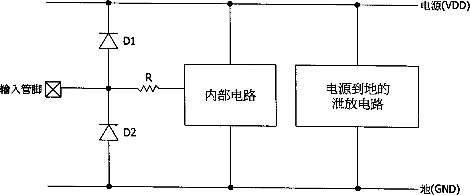
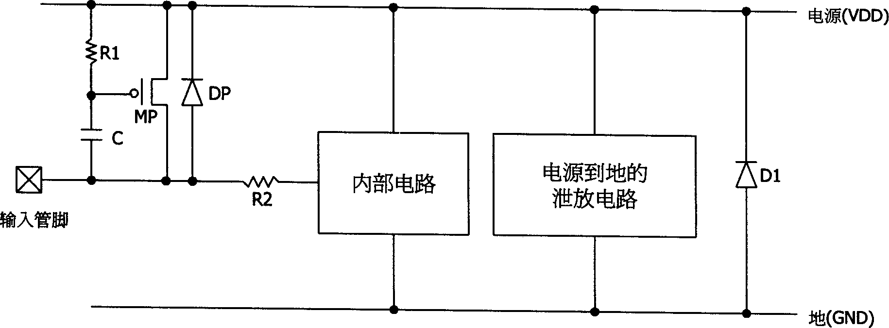
[0013] The present invention proposes an improvement method aiming at that the known protection circuit cannot use the signal input pin lower than the lowest potential in the circuit.

[0014] image 3 Shown is an improved input pin protection circuit of a CMOS integrated circuit, which can realize the electrostatic protection function of the input pin, and does not affect the normal operation of the circuit when the input signal level is lower than 0V. It consists of a PMOS (MP), two resistors R1 and R2, a capacitor C, and a power-to-ground discharge circuit. DP in the figure is the parasitic diode of MP, and D1 is the well in the CMOS integrated circuit (Well) A parasitic diode between the power supply and ground formed with the substrate (Substrate).

[0015] When the integrated circuit using this protection circuit works normally, even if a signal lower than 0V is applied to the input pin, the gate-source voltage (VGS) of MP is still equal to zero and will not conduct, an...


PUM


Abstract

The invention discloses a static protecting method of analog-signal input pin with the lowest potential being common-mode level. It includes a PMOS (MP), two resistances R1 and R2, a capacitance C, and a power supply-ground releasing circuit, to compose a protecting circuit together, R2 set between the pin and the internal circuit, one end of C linked with the pin and R2, respectively, and the other end with R1 and PMOS (MP), respectively. The parasitic diodes are set between the power supply and the ground developed by Well and Substrate in COMS IC.

Description

technical field [0001] The invention relates to an electrostatic protection method for analog signal input pins whose common mode point is lower than the lowest potential in the circuit in a CMOS integrated circuit, especially the electrostatic protection for analog signal input pins whose common mode level is the lowest potential method. Background technique [0002] Generally speaking, for the usual CMOS process, the power supply used by the chip produced by this process is the lowest level GND and the highest level VDD (there are generally 1.8V, 2.5V, 3.3V, 5V, etc. ). Such as figure 1 Shown is a known input pin electrostatic protection circuit, which is composed of two diodes D1, D2, a resistor R and a discharge channel (bleeder circuit) from the power supply to the ground. [0003] For this kind of circuit, when there is static electricity that is positively charged to the power supply VDD applied to the input pin, D1 is forward-conducting, and the positive charge is...

Claims


Application Information

Patent Timeline
IPC IPC(8): H01L23/60
Inventor 丁然
Owner ACTIONS SEMICONDUCTOR
Why Eureka
Try Eureka