Semiconductor apparatus and processing system utilizing the same semiconductor apparatus

A technology for processing systems and semiconductors, which is applied to semiconductor devices, record carriers used in machines, and semiconductor/solid-state device components, etc. It can solve problems such as rising costs, complex chip structures, and wasted performance, and achieve the effect of increasing circuit scale.

Inactive Publication Date: 2004-04-07
RICOH KK
View PDF0 Cites 0 Cited by
  • Summary
  • Abstract
  • Description
  • Claims
  • Application Information

AI Technical Summary

Problems solved by technology

[0005] If the known tolerance technology is applied to the semiconductor device chip used by the above-mentioned read / write device driven by a 3.3V level signal, a 5V level signal can be input, but the chip output signal level is raised from 3.3V to 5V will cause complex chip structure and large chip size, resulting in increased cost
In addition, the low-power-consumption chip manufactured with 0.35μm process regulations and driven by a low voltage of 3.3V will be used as a chip driven by 5V, which will waste more performance

Method used


Image

  • Semiconductor apparatus and processing system utilizing the same semiconductor apparatus
  • Semiconductor apparatus and processing system utilizing the same semiconductor apparatus
  • Semiconductor apparatus and processing system utilizing the same semiconductor apparatus

Examples


Embodiment Construction

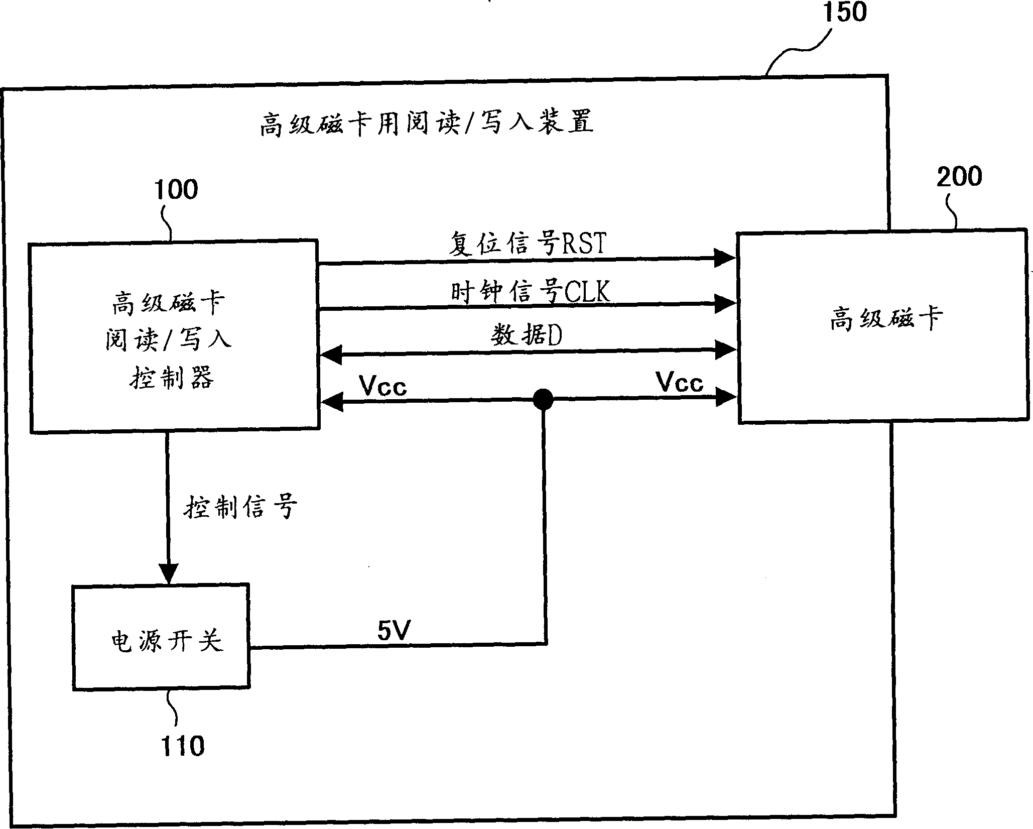
[0029] Hereinafter, as an example of a system for processing signals of different levels, a system composed of an advanced magnetic card and a reading / writing device for advanced magnetic cards will be described, and the system provided with the semiconductor device according to the embodiment of the present invention will be described in detail.

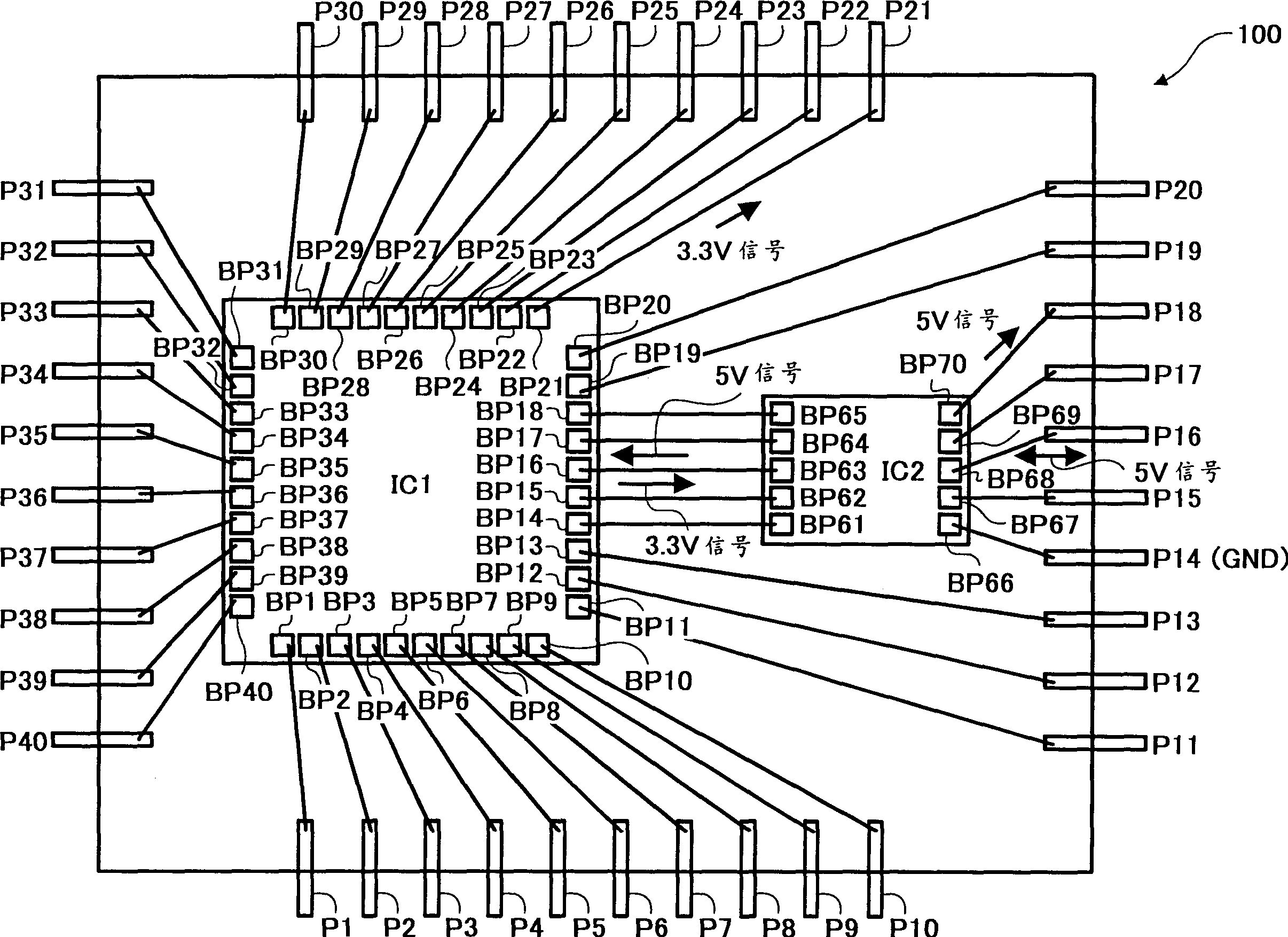
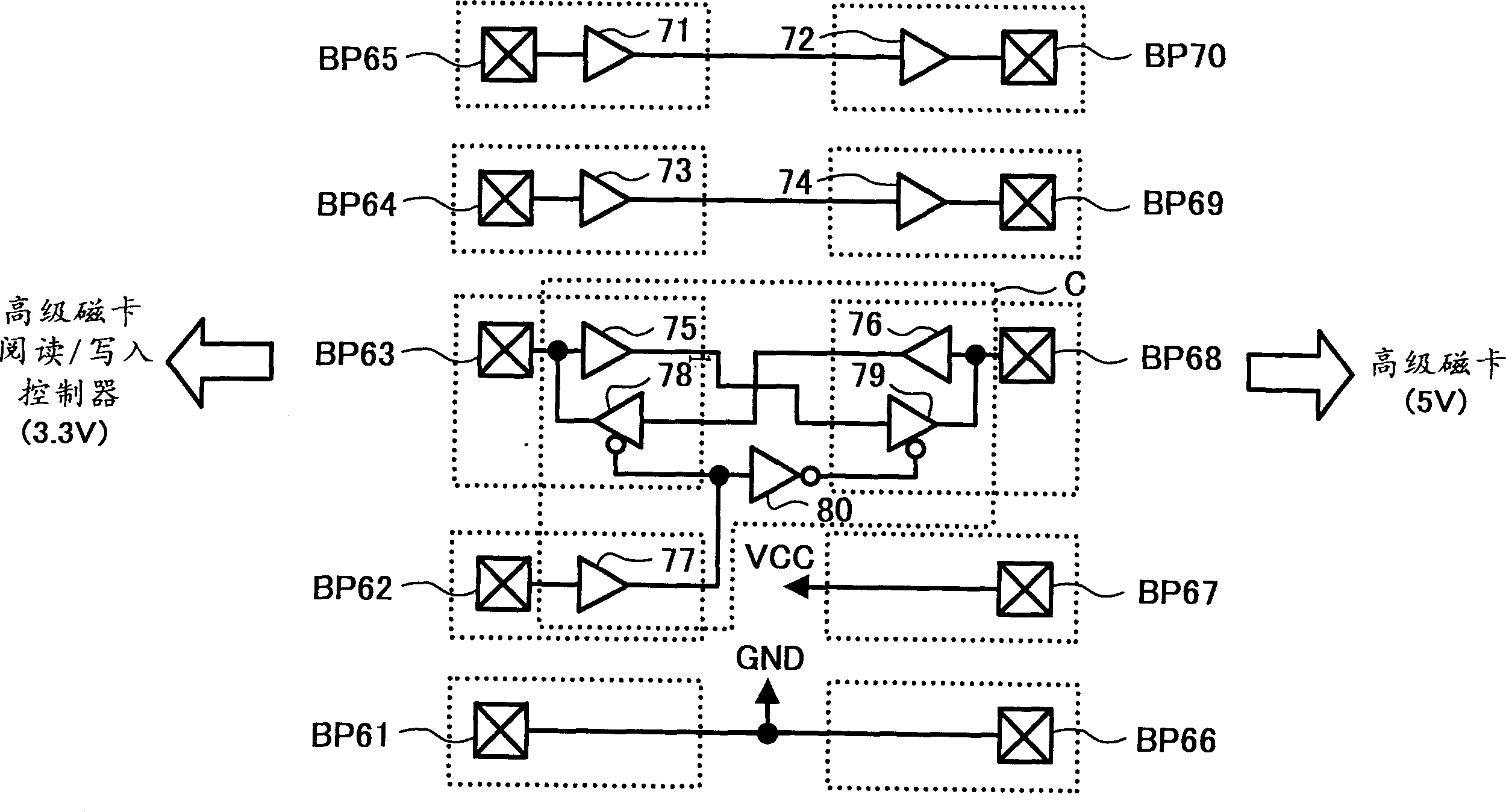
[0030] figure 1 Shows the state where the advanced magnetic card 200 is connected to the advanced magnetic card reading / writing device 150, and when data is written to the advanced magnetic card 200, or data is read from the advanced magnetic card 200, it is used as the reading / writing of the semiconductor device according to the embodiment of the present invention. The write controller 100 sends a turn-on control signal to the power switch 110, and then to the advanced magnetic card 200 and the IC2 embedded in the controller 100 (refer to figure 2 , Will be described in detail later) 5V power supply. After that, the read / write contr...


PUM


Abstract

A semiconductor device which integrates a plurality of semiconductor chips into a single package includes a first semiconductor chip and a second semiconductor chip. The first semiconductor chip includes a plurality of first bonding pads outputting first signals having a first level. The second semiconductor chip includes a plurality of second bonding pads and a plurality of third bonding pads. The plurality of second bonding pads is electrically coupled to a part of the plurality of first bonding pads to receive the first signals having the first level from the first semiconductor chip through the part of the plurality of first bonding pads. The plurality of third bonding pads converts the first signals received through the plurality of second bonding pad into second signals having a second level different from the first level and outputs the second signals through the plurality of third bonding pads.

Description

Technical field [0001] The present invention relates to a semiconductor device corresponding to the input and output of signals of different levels, and a processing system for signals of different levels using the semiconductor device. Background technique [0002] The input / output signal level of the chip included in the semiconductor device becomes lower as the design rule of the chip becomes smaller. For example, when a chip is manufactured with a process rule of 0.5 μm or more, the input and output signal level is mostly above 5V, and when a chip is manufactured with a process rule of 0.35 μm or less, the input and output signal level is set to 3.3V or less. Among the chips manufactured with the 0.35 μm process specification, there are also chips that use well-known tolerance techniques, which can operate normally not only for 3.3V level signals but also for input 5V level signals. [0003] In the following, as an example of a system that processes different signal levels, c...

Claims


Application Information

Patent Timeline
Patent Type & Authority Applications(China)
IPC IPC(8): G06K19/07G06K17/00H01L23/50H01L25/04H01L25/065H01L25/18
CPCH01L2924/01015H01L2924/01023H01L2924/01082H01L2924/19043H01L2224/48137H01L2924/01004H01L24/48H01L2224/48247H01L25/0655H01L2924/01005H01L2924/01033H01L2924/01006H01L23/50H01L2924/01083H01L2224/49175H01L2224/49171H01L24/49H01L2924/13091H01L2924/00014H01L2924/181H01L2224/05554H01L2924/10161H01L2924/10162H01L2924/00H01L2224/45099H01L2224/05599H01L2924/00012
Inventor 山本齐
Owner RICOH KK
Why Eureka
Try Eureka