Supercharge Your Innovation With Domain-Expert AI Agents!

Semiconductor device for reading signal from photod by transistor

A photodiode and semiconductor technology, applied in semiconductor devices, electric solid state devices, components of color TVs, etc., can solve problems such as reducing image quality

Inactive Publication Date: 2004-04-21
FUJITSU SEMICON LTD
View PDF1 Cites 15 Cited by
  • Summary
  • Abstract
  • Description
  • Claims
  • Application Information

AI Technical Summary

Problems solved by technology

Pixels with large junction leakage become white dots, reducing image quality

Method used


Image

  • Semiconductor device for reading signal from photod by transistor
  • Semiconductor device for reading signal from photod by transistor
  • Semiconductor device for reading signal from photod by transistor

Examples


Embodiment Construction

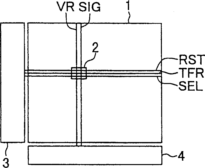
[0036] Figure 1A A block diagram of a four-transistor solid-state imaging device (image sensor) according to the first embodiment of the present invention is shown. A plurality of pixels 2 are arranged in a matrix in the imaging area. Corresponding to each pixel row, a reset signal line RST, a transfer signal line TFR, and a selection line SEL are provided. Corresponding to each pixel column, a signal readout line SIG and a reset voltage supply line VR are provided.

[0037] The row selection circuit 3 regularly sends electrical signals to the reset signal line RST, the transfer signal line TFR and the selection line SEL, which will be introduced later. An imaging signal is input from each pixel 2 to a readout circuit 4 via a signal readout line SIG.

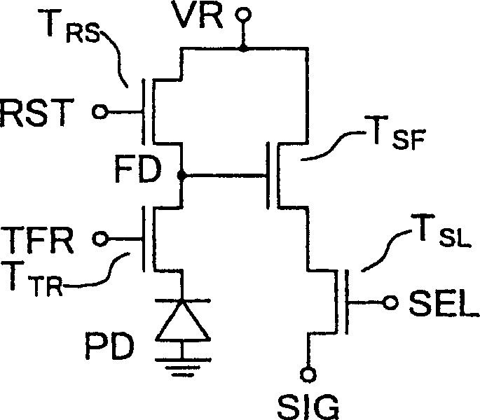
[0038] Figure 1B is the equivalent circuit diagram of a pixel. A pixel consists of photodiode PD, transfer transistor T TR , reset transistor T RS , source follower transistor T SF and the selection transistor T SL . T...


PUM


Abstract

Pixels are disposed on a semiconductor substrate in a matrix shape. Each pixel includes a photodiode, a reset transistor, a source follower transistor and a select transistor. An active region in which the photodiode and transistors are disposed includes a first area in which the photodiode is disposed and a second area having an are elongated in a first direction. Each of the gate electrodes of the reset transistor, source follower transistor and select transistor crosses the area, elongated in the first direction, of the second area. An intra-pixel wiring line interconnects the drain region of the reset transistor and the gate electrode of the source follower transistor.

Description

[0001] Cross References to Related Applications [0002] This application is based on Japanese Patent Application No. 2002-251265 filed on August 29, 2002, the contents of which are incorporated herein by reference. technical field [0003] The present application relates to a semiconductor device that reads an electrical signal of each of a plurality of pixels provided on a semiconductor substrate to a signal reading line by means of a transistor, and the electrical signal is photoelectrically converted by a photodiode of the pixel. Background technique [0004] A solid-state imaging device (image sensor) manufactured according to a complementary MOS (CMOS) process usually uses an active pixel sensor (APS) in which a pixel is composed of: a photodiode for photoelectric conversion; a reset transistor to be applied to the photodiode; a source follower transistor that converts the signal charge of the photodiode into a voltage signal and outputs it; and a selection transistor ...

Claims


Application Information

Patent Timeline
Patent Type & Authority Applications(China)
IPC IPC(8): H01L27/146H04N25/00
CPCH01L27/14603H01L27/14632H01L27/14687H01L27/14689H01L27/146
Inventor 大川成实
Owner FUJITSU SEMICON LTD
Features
  • R&D
  • Intellectual Property
  • Life Sciences
  • Materials
  • Tech Scout
  • Unparalleled Data Quality
  • Higher Quality Content
  • 60% Fewer Hallucinations
Learn More