Appts. and method for creating ultra-clean mini-environment through localized air flow augentation

An air flow, local technology, applied in the field of semiconductor substrate processing equipment, can solve the problems of cost reduction, qualified rate, pollution of two chambers, etc.

Inactive Publication Date: 2004-05-26
LAM RES CORP
View PDF0 Cites 4 Cited by
  • Summary
  • Abstract
  • Description
  • Claims
  • Application Information

AI Technical Summary

Problems solved by technology

These particles can create defects in the semiconductor circuits fabricated on them, causing additional costs and lower yields
Occasionally, particulates migrate through open tank valves, causing potential contami

Method used


Image

  • Appts. and method for creating ultra-clean mini-environment through localized air flow augentation
  • Appts. and method for creating ultra-clean mini-environment through localized air flow augentation
  • Appts. and method for creating ultra-clean mini-environment through localized air flow augentation

Examples


Embodiment Construction

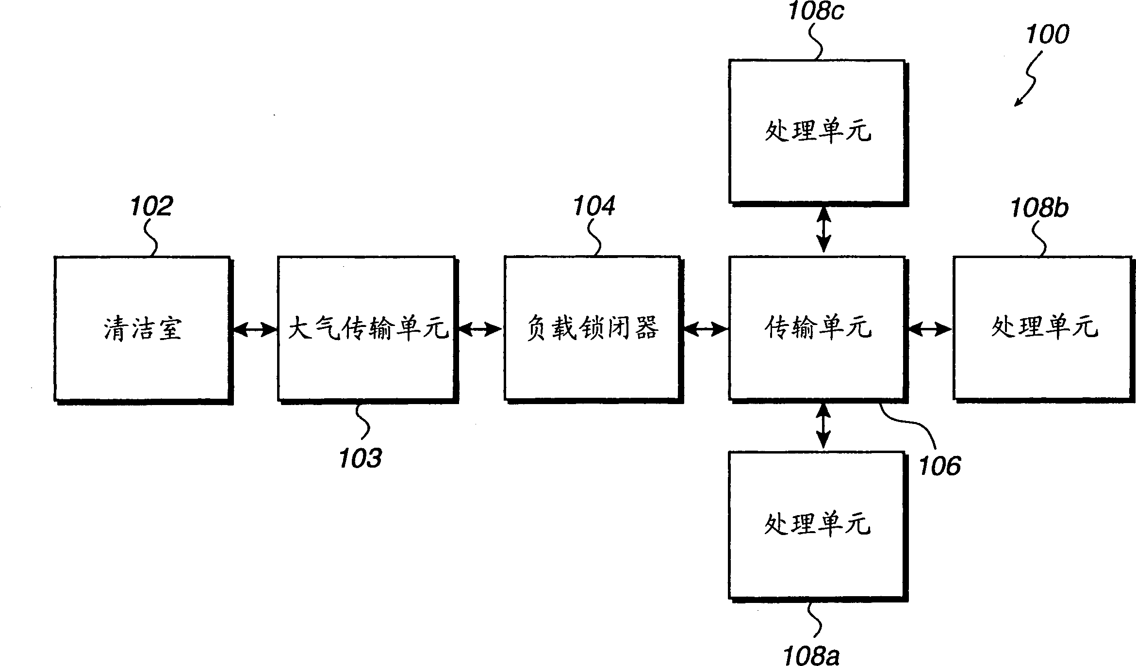
[0024] The invention is used for providing a local ultra-clean microenvironment during wafer processing. In terms used herein, wafer and substrate are interchangeable. Preferably, the mini-environment is configured to include a purge gas flow regime in the vicinity of the particle generation device to purge particles from the wafer or wafer transport path. It will be apparent, however, to one skilled in the art that the present invention may be practiced without some or all of these specific details. In addition, well known process operations have not been described in detail in order not to obscure the present invention.

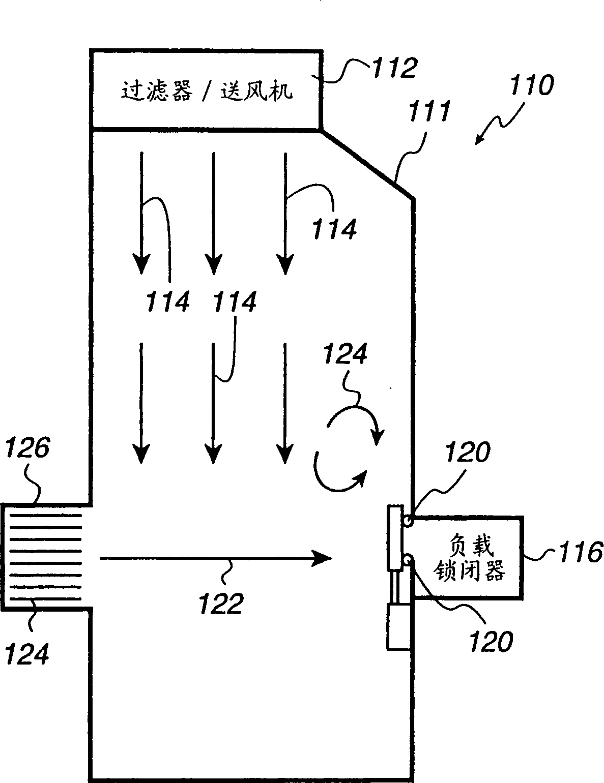
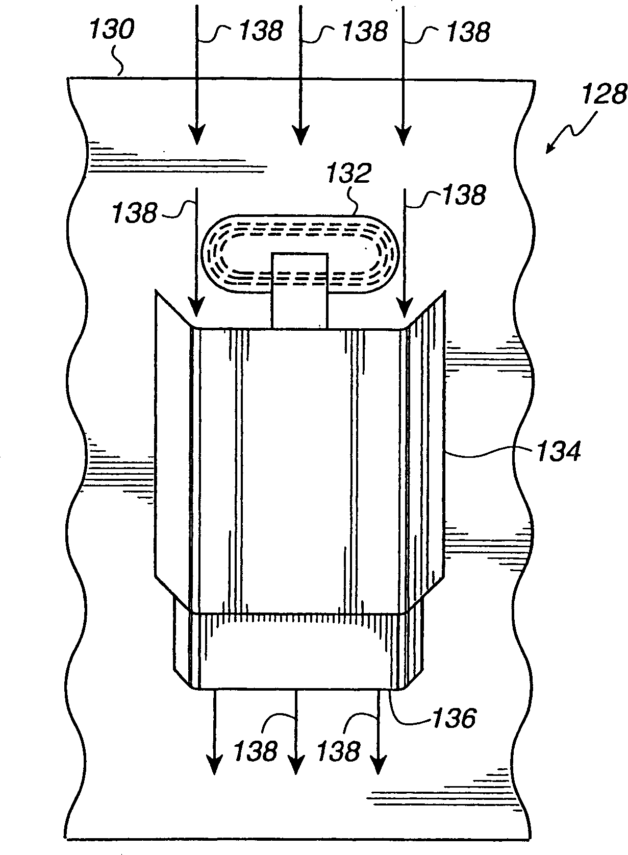
[0025] figure 2 A transfer channel with localized airflow enhancement according to one embodiment of the present invention is shown schematically at 128 . In schematic view 128, chamber wall 130 contains an aperture covered by slit valve 132 shown in the closed position. It will be appreciated that the slot valve 132 in the closed position isolates the...


PUM


Abstract

A method for creating a reduced particle environment in a localized area of a mechanically active transport interface is provided. The augmentation of the air flow results in a sweeping air flow to remove particles in and around the desired area. The augmented air, flow will eliminate static or turbulent air flow regions and assist in removing potential particles from the vicinity of the substrate. This will prevent particles from being deposited on substrates thus fostering higher yields and improved quality.

Description

technical field [0001] The present invention generally relates to semiconductor substrate processing equipment, and more specifically, relates to providing a local ultra-clean microenvironment for substrate processing. Background technique [0002] In the manufacture of semiconductor devices, processing equipment is highly automated in order to expedite transfer between processing steps. For automation, there are a large number of moving mechanical equipment, such as automatic machinery and automatic doors. Any moving mechanical device can be a particle generator. The generated particles can deposit on the substrate in the area near the moving device. In addition, these particles are carried into the gas flow regime within the processing unit, thereby depositing on any wafers or substrates within the processing unit. The generated particles can cause substantial damage to the semiconductor circuits formed on the wafer. For example, particles deposited on a wafer may be t...

Claims


Application Information

Patent Timeline
IPC IPC(8): H01L21/00
CPCY10S414/14H01L21/67017B65G49/07H01L21/02H01L21/68
Inventor 哈兰·I·霍斯戴维·E·雅各布
Owner LAM RES CORP
Why Eureka
Try Eureka